


| Product model | JFTSM-SFP28-25-LWD-40-LCD | Manufacturer brand | JFOPT |
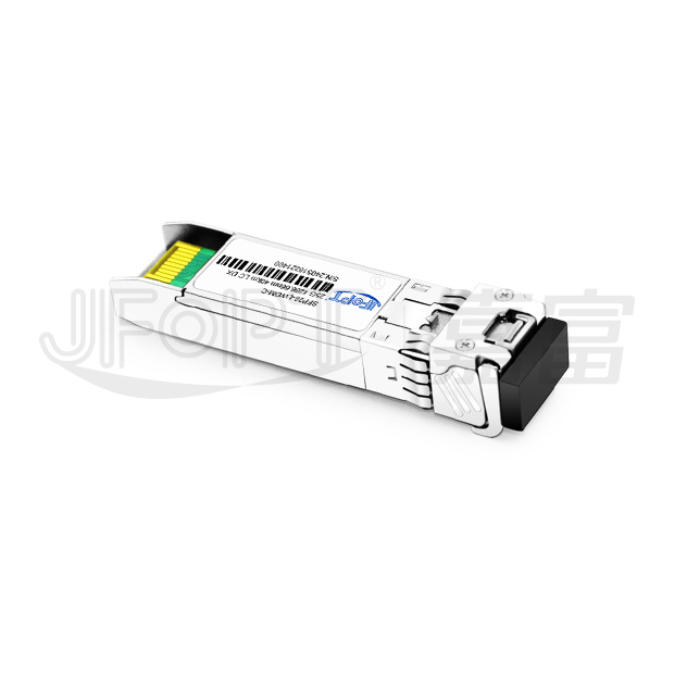
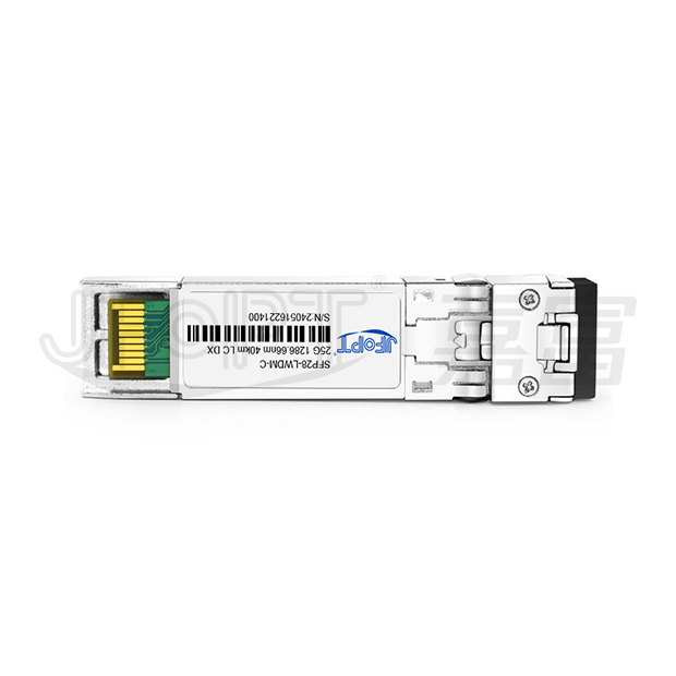
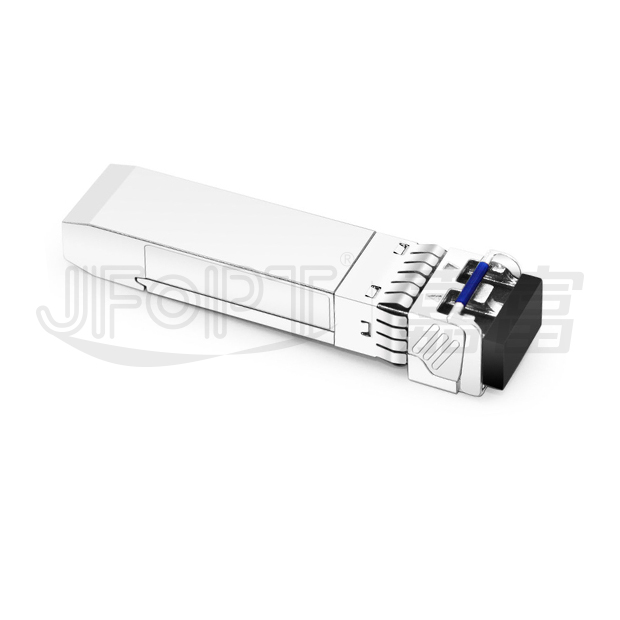
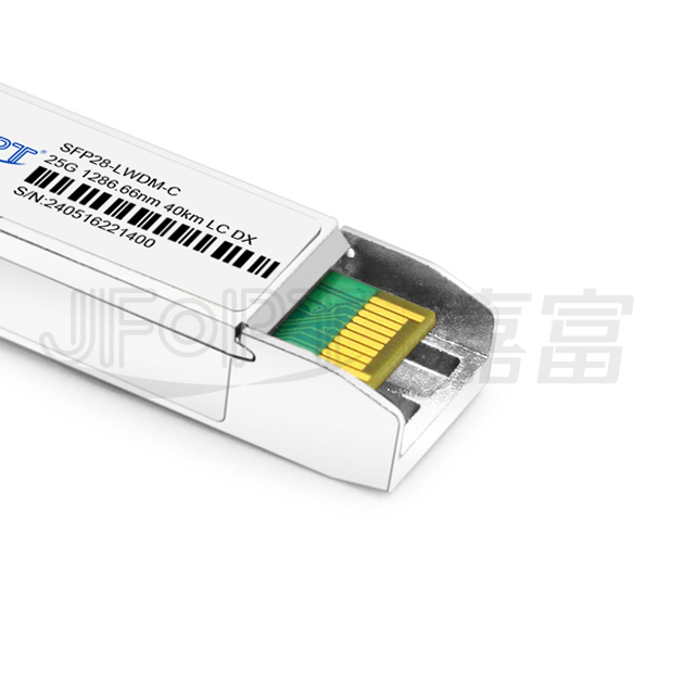
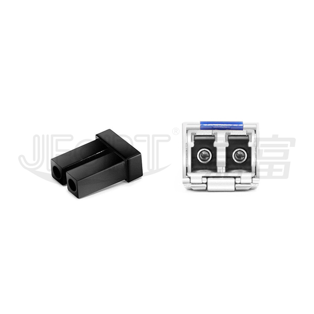
| Package type | SFP28 | Optical connector | Duplex LC |
| Max data rate | 25.78G | Channel data rate | - |
| Effective transmission distance | 40km | ||
| Wavelength | 1286.66nm
1291.10nm
1295.56nm
1300.05nm
1304.58nm
1309.14nm
|
Operating voltage | 3.3V |
| Fiber type | SMF | Core size | 9/125 |
| Transmitter type | EML LWDM | Receiver type | APD |
| TX power | -2~6dBm | Receiver sensitivity | <-19dBm |
| Digital optical monitoring(DOM) | YES | Receiver overload | - |
| Power consumption | 1.5W | Protocols | SFF-8431, SFF-8472, IEEE 802.3CC |
| Operating temperature(Commercial) | 0℃~+70℃ | Storage temperature(Commercial) | -40℃~+85℃ |
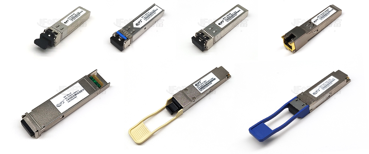
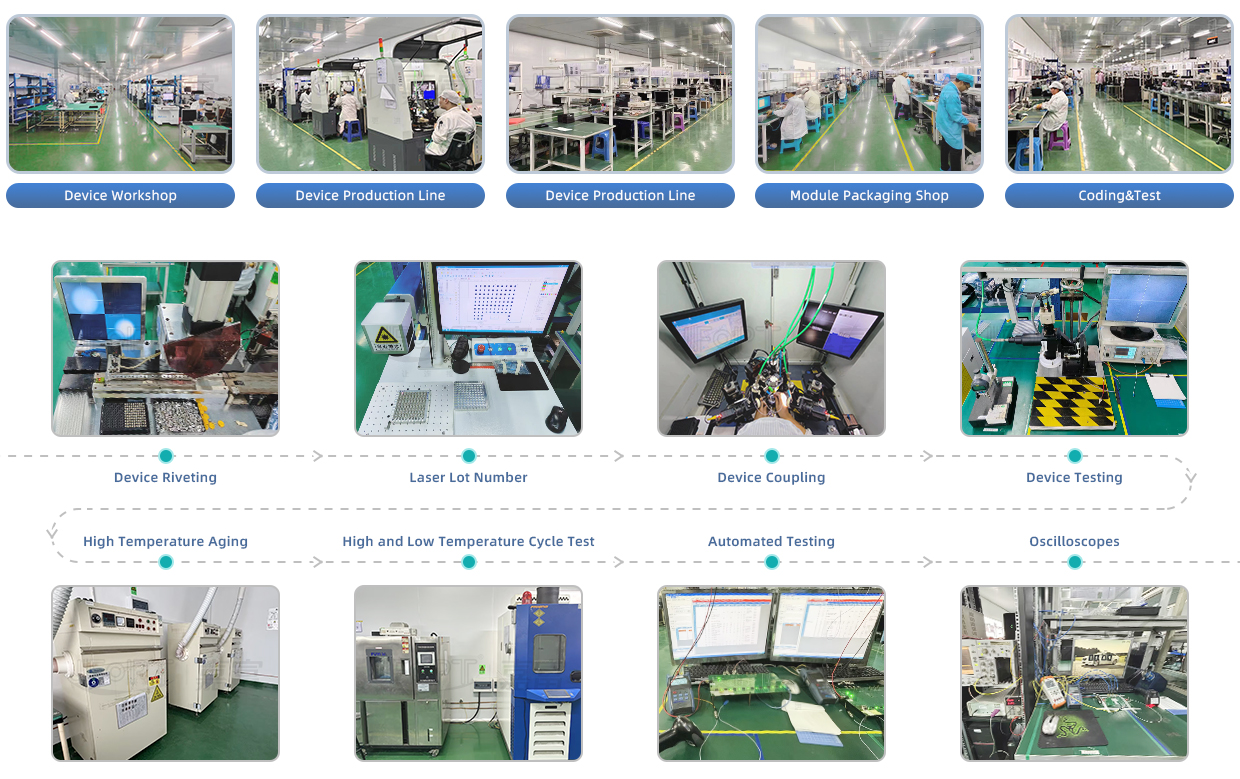
JFOPT continues to invest in optical transceiver production, covering a full range of optical transceiver such as 1*9, SFP, 10G, 25G, 100G, 200G, 400G, 800G GPON/EPON/XG/XGSPON OLT transceiver. At the same time, our company provides TOSA, ROSA, BOSA semi-finished device solutions for the downstream peer. JFOPT's production line has a daily production capacity of 10,000 optical transceivers and 20,000 optical devices. In addition, JFOPT's optical transceiver have industry-leading high temperature resistance and anti-interference capability, and are widely used in computing centers, operators, traffic security, power facilities and other industries.
The JFOPT SFP28 25G LWDM 40km LC DX transceiver is a compact and high-performance optical module designed for 25GBASE-ER Ethernet applications. It converts 25Gbps serial CML electrical signals into serial optical data and ensures compliance with the 25GBASE-ER standard.Equipped with an EML transmitter and an APD receiver, this transceiver delivers exceptional performance for single-mode fiber (SMF) links up to 40km. It adheres to SFF-8431, SFF-8432, and IEEE 802.3CC standards, offering reliable and consistent functionality.Digital diagnostic monitoring is accessible via a 2-wire serial interface, as defined by the SFF-8472 specification. The fully compliant SFP28 form factor supports hot pluggability, simplifies optical port upgrades, and minimizes EMI emissions, making it an ideal solution for high-speed network environments.
| 25.78Gb/s bit rates | Hot-pluggable | ||||||||
| EML transmitter, APD photo-detector | Up to 40km on SMF | ||||||||
| Operating case temperature range: 0~ 70°C | 2-wire interface for management specifications compliant with SFF 8472 digital diagnostic monitoring interface for optical transceivers | ||||||||
| Duplex LC connector | Power supply :+3.3V | ||||||||
| Cost effective SFP28 solution, enables higher port densities and greater bandwidth | Low power consumption<1.5W |
| High-speed storage area networks | Computer cluster cross-connect | |||||||
| Custom high-speed data pipes | Inter rack connection | |||||||
| WDM system | ||||||||

| Parameter | Symbol | Min. | Typ. | Max. | Unit | Ref. | |||
| Storage temperature | TS | -40 | - | +85 | ℃ | - | |||
| Case operating temperature | TA | 0 | - | 70 | ℃ | - | |||
| Maximum supply voltage | VCC | 0 | - | 3.6 | V | - | |||
| Relative humidity | RH | 5 | - | 95 | % | - | |||
| Parameter | Symbol | Min. | Typ. | Max. | Unit | Ref. | |||
| Supply voltage | VCC | 3.135 | - | 3.465 | V | - | |||
| Supply current | ICC | - | - | 606 | mA | - | |||
| Power consumption | P | - | - | 2 | W | - | |||
| Data rate | R | - | 25.78 | - | Gb/s | - | |||
Transmitter section: |
|||||||||
| Input differential impedance | Rin | - | 100 | - | Ω | 1 | |||
| Tx input single ended DC voltage tolerance (ref VeeT) | V | -0.3 | - | 4 | V | - | |||
| Differential input voltage swing | Vin,pp | 180 | - | 700 | mV | 2 | |||
| Transmit disable voltage | VD | 2 | - | VCC | V | - | |||
| Transmit enable voltage | VEN | Vee | - | Vee+0.8 | V | - | |||
Receiver section: |
|||||||||
| Single ended output voltage tolerance | V | -0.3 | - | 4 | V | - | |||
| Rx output diff voltage | VO | 150 | - | 900 | mV | - | |||
| Rx output rise and fall time | Tr/Tf | 9.5 | - | - | ps | 3 | |||
| LOS fault | VLOS fault | 2 | - | VCCHOST | V | 4 | |||
| LOS normal | VLOS norm | Vee | - | Vee+0.8 | V | 4 | |||
| Notes: 1.Connected directly to TX data input pins. AC coupling from pins into laser driver IC. 2.Per SFF-8431 Rev 3.0 3.20%~80% 4.LOS is an open collector output. Should be pulled up with 4.7k – 10kΩ on the host board. Normal operation is logic 0; loss of signal is logic 1. Maximum pull-up voltage is 5.5V. |
|||||||||
| Parameter | Symbol | Min. | Typ. | Max. | Unit | Ref. | |||
Transmitter section: |
|||||||||
| Center Wavelength | λt | 1285.51 | 1286.66 | 1287.81 | nm | - | |||
| 1289.95 | 1291.1 | 1292.25 | |||||||
| 1294.41 | 1295.56 | 1296.71 | |||||||
| 1298.9 | 1300.05 | 1301.2 | |||||||
| 1303.43 | 1304.58 | 1305.73 | |||||||
| 1307.99 | 1309.14 | 1310.29 | |||||||
| spectral width | △λ | - | - | 1 | nm | - | |||
| Average optical power | Pavg | -2.0 | - | +6 | dBm | 1 | |||
| Laser off power | Poff | - | - | -30 | dBm | - | |||
| Extinction ratio | ER | 4 | - | - | dB | - | |||
| Receiver section: | - | - | - | - | - | - | |||
| Center wavelength | λr | 1295 | - | 1325 | nm | - | |||
| Receiver sensitivity(OMA) | Sen | - | - | -19 | dBm | 2 | |||
| Stressed sensitivity(OMA) | Sen2 | - | - | -16.5 | dBm | 2 | |||
| Los sssert | LOSA | -30 | - | - | dBm | - | |||
| Los dessert | LOSD | - | - | -20 | dBm | - | |||
| Los hysteresis | LOSH | 0.5 | - | 5 | dB | - | |||
| Overload | Sat | -6 | - | - | dBm | 3 | |||
| Receiver reflectance | Rrx | - | - | -12 | dB | - | |||
| Notes: 1.Average power figures are informative only, per IEEE802.3CC. 2.Conditions of stressed receiver tests per IEEE802.3CC. At 5E-5 BER. 3.Receiver overload specified in OMA and under the worst comprehensive stressed condition. |
|||||||||
| Parameter | Symbol | Min. | Typ. | Max. | Unit | ||||
| TX_disable assert time | t_off | - | - | 100 | us | ||||
| TX_disable negate time | t_on | - | - | 2 | ms | ||||
| Time to initialize include reset of TX_FAULT | t_int | - | - | 300 | ms | ||||
| TX_FAULT from fault to assertion | t_fault | - | - | 1 | ms | ||||
| TX_disable time to start reset | t_reset | 10 | - | - | us | ||||
| Receiver loss of signal assert time | TA,RX_LOS | - | - | 100 | us | ||||
| Receiver loss of signal de assert time | Td,RX_LOS | - | - | 100 | us | ||||
| Rate-select chage time | t_ratesel | - | - | 10 | us | ||||
| Serial ID clock time | t_serial-clock | - | - | 100 | kHz | ||||
| Data Address | Parameter | Accuracy | Unit | ||||||
| 96-97 | Transceiver internal temperature | ±3.0 | ℃ | ||||||
| 98-99 | VCC3 internal supply voltage | ±3.0 | % | ||||||
| 100-101 | Laser bias current | ±10 | % | ||||||
| 102-103 | Tx output power | ±2.0 | dBm | ||||||
| 104-105 | Rx input power | ±2.0 | dBm | ||||||
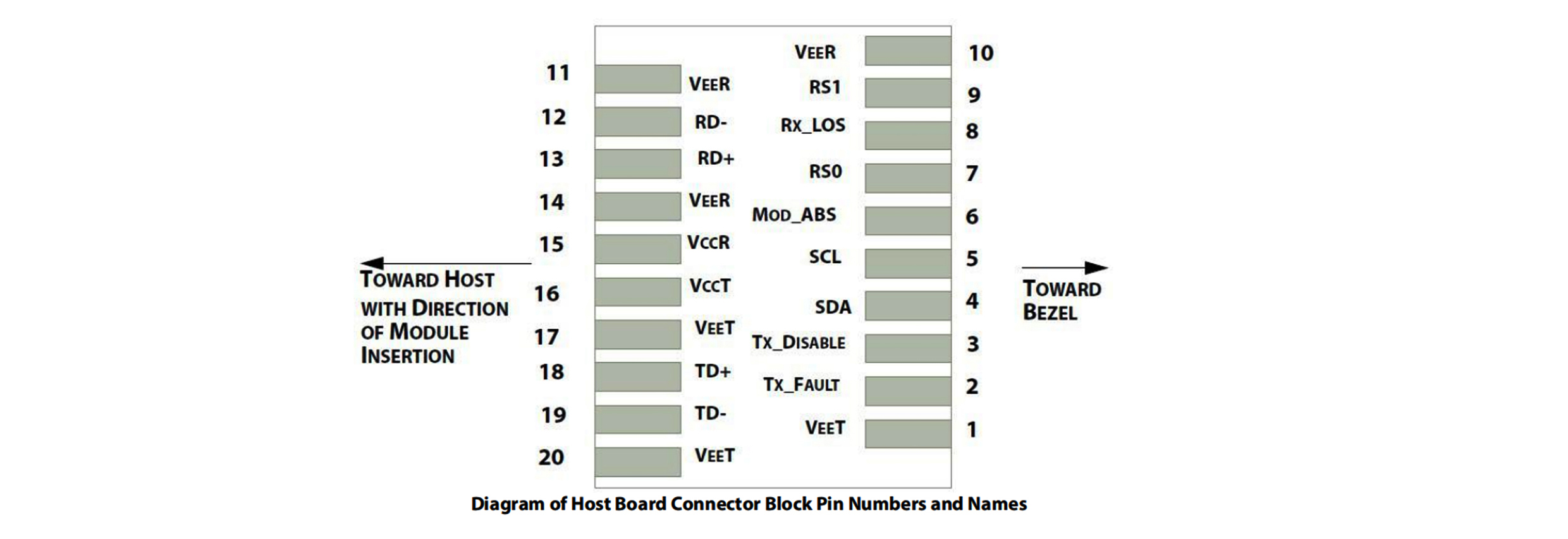
| Pin | Name | Function | Notes | ||||||
| 1 | VeeT | Module transmitter ground | 1 | ||||||
| 2 | TX fault | Module transmitter fault | 2 | ||||||
| 3 | TX disable | Transmitter disable; Turns off transmitter laser output | 3 | ||||||
| 4 | SDL | 2 wire serial interface data input/output (SDA) | 4 | ||||||
| 5 | SCL | 2 wire serial interface clock input (SCL) | 4 | ||||||
| 6 | MOD_ABS | Module absent, connect to VeeR or VeeT in the module | 2 | ||||||
| 7 | RS0 | Rate select0, optionally control SFP+ receiver. When high, input data rate >4.5Gb/ s; when low, input data rate <=4.5Gb/s | - | ||||||
| 8 | LOS | Receiver Loss of signal indication | - | ||||||
| 9 | RS1 | Rate select0, optionally control SFP+ transmitter. When high, input data rate >4.5Gb/s; when low, input data rate <=4.5Gb/s | - | ||||||
| 10 | VeeR | Module receiver ground | 1 | ||||||
| 11 | VeeR | Module receiver ground | 1 | ||||||
| 12 | RD- | Receiver inverted data out put | - | ||||||
| 13 | RD+ | Receiver non-inverted data out put | - | ||||||
| 14 | VeeR | Module receiver ground | 1 | ||||||
| 15 | VccR | Module receiver 3.3V supply | - | ||||||
| 16 | VccT | Module transmitter 3.3V supply | - | ||||||
| 17 | VeeT | 1 | |||||||
| 18 | TD+ | Transmitter non-inverted data out put | - | ||||||
| 19 | TD- | - | |||||||
| 20 | VeeT | Module transmitter ground | 1 | ||||||
| Notes: 1.The module ground pins shall be isolated from the module case. 2.This pin is an open collector/drain output pin and shall be pulled up with 4.7K-10Kohms to Host_Vcc on the host board. 3.This pin shall be pulled up with 4.7K-10Kohms to VccT in the module. 4.This pin is an open collector/drain output pin and shall be pulled up with 4.7K-10Kohms to Host_Vcc on the host board. |
|||||||||


 Ann
Ann


