


|
Product model
|
JFTSM-SFP+8.5-13-2(LRL)/10(LR)/20(ELR)-LCD
|
Manufacturer brand
|
JFOPT
|
|
Package type
|
SFP+
|
Interface type
|
LC Duplex
|
|
Max data rate
|
8.5Gbps
|
Channel data rate
|
8.5Gbps
|
|
Effective transmission distance
|
1.4km,10km,20km
|
||
|
Wavelength
|
1310nm
|
Operating voltage
|
3.3V
|
|
Fiber type
|
SMF
|
Core size
|
9/125
|
|
Transmitter type
|
FP-LD,DFB
|
Receiver type
|
IDP
|
|
TX power
|
-8.2~0.5dBm,-4~0dBm
|
Receiver sensitivity
|
-14dBm,-15dBm
|
|
Digital optical monitoring(DOM)
|
YES
|
Receiver overload
|
0.5dBm
|
|
Power consumption
|
<1.0W
|
Protocols
|
MSA SFP+ SFF-8431
|
|
Operating temperature(Commercial)
|
0℃~+70℃
|
Storage temperature(Commercial)
|
-40℃~+85℃
|
|
Operating temperature(Industrial)
|
-40℃~+85℃
|
Storage temperature(Industrial)
|
-40℃~+85℃
|
JFOPT continues to invest in optical transceiver production, covering a full range of optical transceiver such as 1*9, SFP, 10G, 25G, 100G, 200G, 400G, 800G GPON/EPON/XG/XGSPON OLT transceiver. At the same time, our company provides TOSA, ROSA, BOSA semi-finished device solutions for the downstream peer. JFOPT's production line has a daily production capacity of 10,000 optical transceivers and 20,000 optical devices. In addition, JFOPT's optical transceiver have industry-leading high temperature resistance and anti-interference capability, and are widely used in computing centers, operators, traffic security, power facilities and other industries.
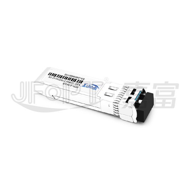
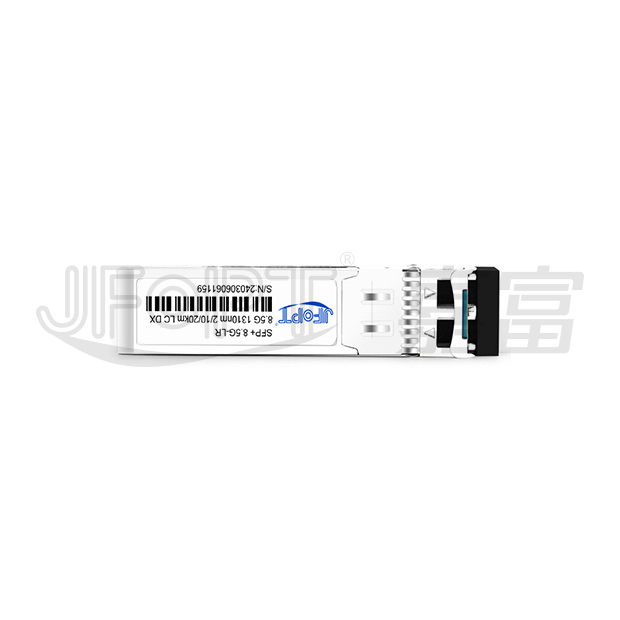
The JFOPT SFP+ 8.5G 1310nm 1.4/10/20km LC DX single mode transceiver is a compact, pluggable module designed for high-speed optical data communication. Featuring an SFP+ 20-pin connector, it supports hot plug capability. This module is optimized for single-mode fiber and operates at a nominal wavelength of 1310nm. The transmitter incorporates a 1310nm multiple quantum well FP laser, complying with Class 1 laser safety standards as per IEC-60825. The receiver utilizes an integrated InGaAs detector preamplifier (IDP) within the optical header, paired with a limiting post-amplifier IC for enhanced signal processing.
| Operating data rate up to 8.5Gbps | 1310nm FP-LD transmitter | ||||||||
| Distance up to 20km | Single 3.3V power supply and TTL logic interface | ||||||||
| Compliant with SFP MSA |
Operating case temperature:
Extended:-10℃~70℃
Industrial: -40℃~85℃
|
||||||||
| Duplex LC connector interface | Hot pluggable | ||||||||
| Power dissipation < 1.0W | Compliant with MSA SFP+ Specification SFF-8431 |
| 8G fiber channe | OBSAI rates 6.144 Gb/s, 3.072 Gb/s, 1.536 Gb/s, 0.768Gb/s | ||||||||
| CPRI rates 7.373Gb/s, 6.144 Gb/s, 4.915 Gb/s, 2.458 Gb/s, 1.229 Gb/s, 0.614Gb/s | Other optical links | ||||||||
| 8XFC at 8.5Gbps;4XFC at 4.25Gpbs;2XFC at 2.125Gpbs;1XFC at 1.0625Gbps |

| Part No. | Data Rate | Laser | Fiber Type | Distance | Optical Interface | Temp. | DDMI | |
| JFTSM-SFP+8.5-13-2(LRL)/10(LR)/20(ELR)-LCD | 0.614Mbps~8.5Gbps | 1310nm DFP | SMF | 1.4km | LC | Standard | YES | |
| 0.614Gbps to 8.5Gbps |
1310nm DFB | SMF | 10km | LC | Standard | YES | ||
| 0.614Gbps to 8.5Gbps |
1310nm DFB | SMF | 20km | LC | Standard | YES | ||
| Parameter | Symbol | Min. | Max. | Unit | ||||
| Storage temperature | TS | -40 | +85 | °C | ||||
| Supply voltage | VCC | -0.5 | 3.6 | V | ||||
| Input voltage | Vin | -0.5 | Vcc | V | ||||
| Output current | Io | - | 50 | mA | ||||
| Parameter | Symbol | Min. | Typical | Max. | Unit | |||
| Operating case temperature | TC | Standard | 0 | - | +70 | °C | ||
| Industrial | -40 | - | +85 | |||||
| Power supply voltage | VCC | 3.15 | 3.3 | 3.45 | V | |||
| Power supply current | ICC | - | - | 300 | mA | |||
| Surge current | ISurge | - | - | +30 | mA | |||
| Parameter | Symbol | Min. | Typ. | Max | Unit | Notes | ||
Transmitter |
||||||||
| CML Inputs(Differential) | Vin | 150 | - | 1200 | mVpp | AC coupled inputs | ||
| Input AC common mode voltage | - | 0 | - | 25 | mV | RMS | ||
| Input impedance(Differential) | Zin | 85 | 100 | 115 | ohm | Rin > 100 kohms @ DC | ||
| Differential Input S-parameter | SDD 11 | - | - | -10 | dB | |||
| Differential to common mode conversion | SCD 11 | - | - |
-10
|
dB
|
|||
| Tx_DISABLE input voltage–high | - | 2.0 | - | Vcc+0.3 | V | |||
| Tx_DISABLE input voltage–low | - | 0 | - | 0.8 | V | |||
| Tx_FAULT output voltage–high | - | 2.0 | - | Vcc | V | Io = 400µA; Host Vcc | ||
| Tx_FAULT output voltage–low | - | - | 0.5 | V | Io = -4.0mA | |||
Receiver |
||||||||
| CML outputs (Differential) | Vout | 350 | - | 700 | mVpp | AC coupled outputs | ||
| Mode voltage | - | 0 | - | 15 | mV | RMS | ||
| Output impedance(Differential) | Zout | 90 | 100 | 110 | ohm | - | ||
| Differential output S-parameter | SD22 | - | - | - 10 | dB | - | ||
| Rx_LOS output voltage–high |
- | 2.0 | - | Vcc+0.3 | V | lo = 400µA; Host Vcc | ||
| Rx_LOS output voltage–low |
- | 0 | - | 0.8 | V | lo = -4.0mA | ||
| MOD_DEF ( 2:0 ) | VoH | 2.5 | - | - | V | With serial ID | ||
| VoL | 0 | - | 0.5 | V | ||||
| Parameter | Symbol | Unit | (SFP+ 8.5G 1310nm 1.4km LC DX) | (SFP+ 8.5G 1310nm 10km LC DX) | (SFP+ 8.5G 1310nm 20km LC DX) | ||||||||
| Min. | Typical | Max. | Min. | Typical | Max. | Min. | Typical | Max. | |||||
| 9µm core diameter SMF supported distance | - | km | - | 1.4 | - | - | - | 10 | - | - | 20 | ||
| Data Rate | - | Gbps | 0.614 | - | 8.5 | 0.614 | - | 8.5 | 0.614 | - | 8.5 | ||
Transmitter |
|||||||||||||
| Centre wavelength | λC | nm | 1260 | 1310 | 1355 | 1270 | 1310 | 1355 | 1270 | 1310 | 1355 | ||
| Spectral width | Δλ | nm | - | - | - | - | - | 1 | - | - | 1 | ||
| Side mode suppression ratio | SMSR | dB | - | - | 3 | 30 | - | - | 30 | - | - | ||
| Average output power | Pout | dBm | -8.2 | - | 0.5 | -8.2 | - | +0.5 | -4 | - | 0 | ||
| Extinction ratio | ER | dB | 3.5 | - | - | 3.5 | - | - | 3.5 | - | - | ||
| Transmitter dispersion penalty | TDP | dB | - | - | 5.2 | - | - | - | - | - | - | ||
| Input differential impedance | ZIN | Ω | 90 | 100 | 110 | - | - | - | - | - | - | ||
| Average power of OFF transmitter | Poff | dBm | - | - | 10 | - | - | -30 | - | - | -30 | ||
| TX disable assert time | t_off | us | - | - | 1 | - | - | 10 | - | - | 10 | ||
| TX_DISABLE negate time | t_on | ms | 10 | - | - | - | - | 1 | - | - | 1 | ||
| TX_BISABLE time to start reset | t_reset | us | - | - | 300 | 10 | - | - | 10 | - | - | ||
| Time to initialize, include reset of TX_FAULT | t_init | ms | - | - | 100 | - | - | 300 | - | - | 300 | ||
| TX_FAULT from fault to assertion | t_fault | us | - | - | - | - | - | 100 | - | - | 100 | ||
| Total Jitter | TJ | UI(p-p) | - | - | - | - | - | 0.28 | - | - | 0.28 | ||
| Data dependant jitter | DDJ | UI(p-p) | - | - | - | - | - | 0.1 | - | - | 0.1 | ||
| Uncorrelated jitter | UJ | RMS | - | - | - | - | - | 0.023 | - | - | 0.023 | ||
Receiver |
|||||||||||||
| Centre wavelength | λ | nm | 1260 | - | 1565 | 1260 | - | 1565 | 1260 | - | 1565 | ||
| Sensitivity | Pmin | dBm | - | - | -14 | - | - | -15 | - | - | -15 | ||
| Receiver overload | Pmax | dBm | 0.5 | - | - | 0.5 | - | - | 0.5 | - | - | ||
| Optical return loss | ORL | dB | - | - | -12 | - | - | -12 | - | - | -12 | ||
| LOS De-Assert | LOSD | dBm | - | - | -16 | - | - | -17 | - | - | -17 | ||
| LOS Assert | LOSA | dBm | -28 | - | - | -29 | - | - | -29 | - | - | ||
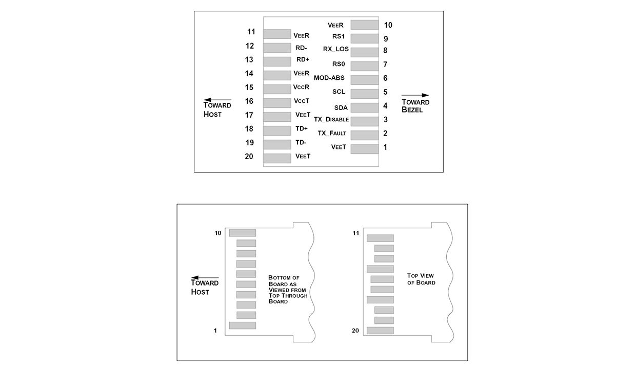
| Pin Num. | Name | Function | Plug Seq. | Notes | ||||
| 1 | VeeT | Transmitter ground | 1 | Note 5 | ||||
| 2 | TX Fault | Transmitter fault indication | 3 | Note 1 | ||||
| 3 | TX Disable |
Transmitter disable | 3 | Note 2, Module disables on high or open | ||||
| 4 | SDA | Module definition 2 | 3 | Data line for serial ID. | ||||
| 5 | SCL | Module definition 1 | 3 | Clock line for serial ID. | ||||
| 6 | MOD-ABS | Module definition 0 | 3 | Note 3 | ||||
| 7 | RS0 | RX rate select(LVTTL). | 3 | No function implement.. | ||||
| 8 | LOS | Loss of signal | 3 | Note 4 | ||||
| 9 | RS1 | TX rate select(LVTTL). | 1 | No function implement.. | ||||
| 10 | VeeR | Receiver ground | 1 | Note 5 | ||||
| 11 | VeeR | Receiver ground | 1 | Note 5 | ||||
| 12 | RD- | Inv. Received data out | 3 | Note 6 | ||||
| 13 | RD+ | Received data out | 3 | Note 7 | ||||
| 14 | VeeR | Receiver ground | 1 | Note 5 | ||||
| 15 | VccR | Receiver power | 2 | 3.3V ± 5%, Note 7 | ||||
| 16 | VccT | Transmitter power | 2 | 3.3V ± 5%, Note 7 | ||||
| 17 | VeeT | Transmitter ground | 1 | Note 5 | ||||
| 18 | TD+ | Transmit data in | 3 | Note 8 | ||||
| 19 | TD- | Inv. Transmit data in | 3 | Note 8 | ||||
| 20 | VeeT | Transmitter ground | 1 | Note 5 | ||||
Notes:


 Ann
Ann


