


|
Product model
|
JFTSM-SFPBD-1.25-1314-055/3/10/20/40/60-LC/SC
|
Manufacturer brand
|
JFOPT
|
|
Package type
|
SFP
|
Optical connector
|
Simplex SC/LC
|
|
Max data rate
|
up to 1.25G
|
Channel data rate
|
-
|
|
Effective transmission distance
|
550M 3/10/20/40/60KM
|
||
|
Wavelength
|
1310nm/1490nm
1490nm/1310nm
|
Operating voltage
|
3.3V
|
|
Fiber type
|
550M MMF
3/10/20/40/60KM SMF
|
Core size
|
550M 50/125µm
3/10/20/40/60KM 9/125µm
|
|
Transmitter type
|
FP/DFB
|
Receiver type
|
IDP
|
|
TX power
|
550M -9.5~-3dbm
3KM -14~-8dbm
10KM -9~-3dbm
20KM -8~-3dbm
40KM -5~0dbm
60KM 0~5dbm
|
Receiver sensitivity
|
550M -21dbm
3/10/20KM -22dbm
40KM -24dbm
60KM -27dbm
|
|
Digital optical monitoring(DDM)
|
YES
|
Receiver overload
|
-3dbm
|
|
Power consumption
|
<1W
|
Protocols
|
SFP MSA SFF-8472
|
|
Operating temperature(Commercial)
|
0℃~+70℃
|
Storage temperature(Commercial)
|
-40℃~+85℃
|
|
Operating temperature(Industrial)
|
-40℃~+85℃
|
Storage Temperature(Industrial)
|
-40℃~+85℃
|
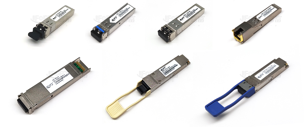
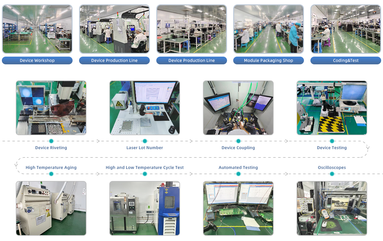
JFOPT continues to invest in optical transceiver production, covering a full range of optical transceiver such as 1*9, SFP, 10G, 25G, 100G, 200G, 400G, 800G GPON/EPON/XG/XGSPON OLT transceiver. At the same time, our company provides TOSA, ROSA, BOSA semi-finished device solutions for the downstream peer. JFOPT's production line has a daily production capacity of 10,000 optical transceivers and 20,000 optical devices. In addition, JFOPT's optical transceiver have industry-leading high temperature resistance and anti-interference capability, and are widely used in computing centers, operators, traffic security, power facilities and other industries.
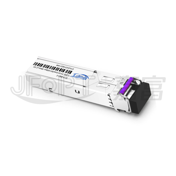
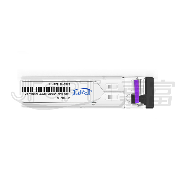
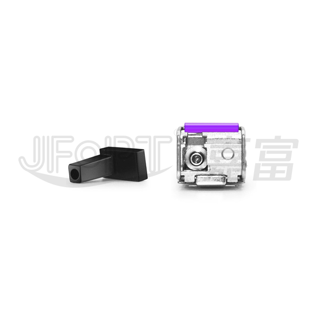
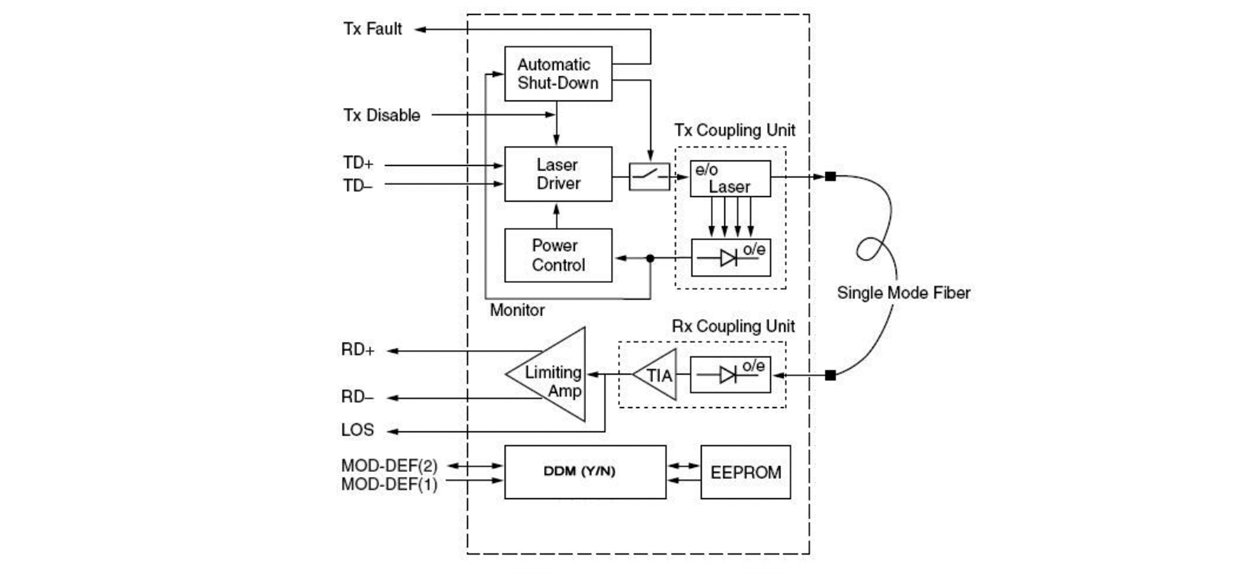
The JFOPT SFPBD-1.25-1314-055/3/10/20/40/60-LC/SC series (SFP BIDI 1.25G 1310/1490nm LC/SC SX Transceiver), a high-performance multi-rate transceiver designed for Gigabit Ethernet fiber communications, features a compact small form-factor pluggable module supporting bi-directional communication over single fiber via a 1310nm/1490nm transmitter paired with a 1490nm/1310nm receiver. Available for transmission distances of 550 meters, 3km, 10km, 20km, 40km, and 60km with a 20-pin SFP connector enabling hot-plug capability for easy installation and maintenance, its transmitter section incorporates a high-quality multiple quantum well A-type/B-type laser compliant with IEC 60825 Class 1 laser safety standards, while the receiver section employs an advanced optical detection system including an integrated B-type/A-type detector preamplifier (IDP) mounted in an optical header and a precision limiting post-amplifier IC to ensure reliable signal reception and processing, with full compliance to SFF-8472 SFP Multi-Source Agreement (MSA) guaranteeing industry-standard compatibility and interoperability for seamless network integration.
| Support 1.25Gbps data links | 550m with 50/125µm MMF | ||||||||
| Up to 3km with 9/125 µm SMF | Up to 10km with 9/125 µm SMF | ||||||||
| Up to 20km with 9/125 µm SMF | Up to 40km with 9/125 µm SMF | ||||||||
| Up to 60km with 9/125 µm SMF | A type: 1310nm FP TX/1490nm RX B type: 1490nm FP TX/1310nm RX |
||||||||
| A type: 1310nm FP TX /1490nm RX B type: 1490nm DFB TX /1310nm RX |
A type: 1310nm DFB TX /1490nm RX B type: 1490nm DFB TX /1310nm RX |
||||||||
| Single 3.3V power supply and TTL logic interface | Hot-pluggable SFP footprint simplex SC/LC connector interface |
| Gigabit ethernet switches and routers | Fiber channel switch infrastructure | |||||||
| Fiber channel links | WDM gigabit ethernet links | |||||||
| Other optical links | ||||||||

| Part No. | Data Rate | Wavelength | Interface | Temp. | DDMI | ||||
| JFTSM-SFPBD-1.25-1314-055-LC/SC | 1.25Gbps | 1310nm/1490nm | SC | Standard | YES | ||||
| 1310nm/1490nm | Industrial | ||||||||
| 1310nm/1490nm | LC | Standard | YES | ||||||
| 1310nm/1490nm | Industrial | YES | |||||||
| JFTSM-SFPBD-1.25-1314-3/10/20/40/ 60-LC/SC |
0.1~1.25Gbps | 1310nm/1490nm | SC | Standard | YES | ||||
| 1310nm/1490nm | Industrial | ||||||||
| 1310nm/1490nm | LC | Standard | YES | ||||||
| 1310nm/1490nm | Industrial | YES | |||||||
| Parameter | Symbol | Min. | Max. | Unit | |||||
| Storage temperature | TS | -4.0 | +85 | ℃ | |||||
| Supply voltage | VCC | -0.5 | 3.6 | V | |||||
| Operating relative humidity | - | - | 95 | % | |||||
Exceeding any one of these values may destroy the device immediately. |
|||||||||
| Parameter | Symbol | Min | Typical | Max | Unit | ||||
| Operating case temperature | Tc |
JFTSM-SFPBD-1.25-1314-055/3/10/20/
40/60/80-LC/SC
|
0 | - | +70 | °C | |||
| -40 | - | +85 | |||||||
| Power supply voltage | Vcc | 3.15 | 3.3 | 3.45 | V | ||||
| Power supply current | Icc | - | - | 300 | mA | ||||
| Date rate | - | - | 1.25 | - | Gbps | ||||
| Parameter | Symbol | Min. | Typ. | Max. | Unit | Notes | |||
Transmitter |
|||||||||
| LVPECL inputs(Differential) | Vin | 400 | - | 2000 | mVpp | AC coupled inputs | |||
| Input impedance (Differential) | Zin | 85 | 100 | 115 | ohm | Rin > 100 kohm @ DC | |||
| TX_dis | Disable | - | 2 | - | Vcc+0.3 | V | - | ||
| Enable | - | 0 | - | 0.8 | - | ||||
| TX_FAULT | Fault | - | 2 | - | Vcc+0.3 | V | - | ||
| Normal | - | 0 | - | 0.5 | - | ||||
Receiver |
|||||||||
| LVPECL outputs (Differential) | Vout | 370 | - | 2000 | mVpp | AC coupled output | |||
| Output impedance(Differential) | Zout | 85 | 100 | 115 | ohms | - | |||
| RX_LOS | LOS | - | 2 | - | Vcc+0.3 | V | - | ||
| Normal | - | 0 | - | 0.8 | V | - | |||
| MOD_DEF ( 0:2 ) | VoH | 2.5 | - | - | V | With serial ID | |||
| VoL | 0 | - | 0.5 | V | |||||
| Parameter | Symbol | Unit | 1310nm FP and PIN, 550m | 1310nm FP and PIN, 3km | 1310nm FP and PIN, 10km | ||||||
| Min. | Typical | Max. | Min. | Typical | Max. | Min. | Typical | Max. | |||
| 50µm Core Diameter MMF | L | km | - | 0.55 | - | - | - | - | - | - | - |
| 9µm Core Diameter SMF | L | km | - | - | - | - | 3 | - | - | 10 | - |
| Data rate | - | Gbps | 100 | 1.063/1.25 | - | - | 1.25 | - | - | - | 1.25 |
Transmitter |
|||||||||||
| Center wavelength | λC | nm | 1260 | 1310 | 1360 | 1270 | 1310 | 1350 | 1270 | 1310 | 1350 |
| Spectral width(RMS) | Δλ | nm | - | - | 4 | - | - | 4 | - | - | 3.5 |
| Average output power | Pout | dBm | -9.5 | - | -3 | -14 | - | -8 | -9 | - | -3 |
| Extinction ratio | ER | dB | 6 | - | - | 6 | - | - | 9 | - | - |
| Rise/Fall time(20%~80%) | tr/tf | ns | - | - | 0.26 | - | - | 0.26 | - | - | 0.26 |
| Total jitter | TJ | ps | - | - | 56.5 | - | - | 260 | - | - | 260 |
| Output optical eye | - | - | Compatible with IEEE 802.3ah-2004 | Compliant with IEEE 802.3z | Compliant with IEEE 802.3-2005/IEEE 802.3.ah | ||||||
| TX disable assert time | t_off | us | - | - | 10 | - | - | 10 | - | - | 10 |
| Pout@TX disable asserted | Pout | dBm | - | - | -45 | - | - | -45 | - | - | -45 |
Receiver |
|||||||||||
| Center wavelength | λC | nm | 1450 | 1490 | 1530 | 1450 | 1490 | 1530 | 1450 | 1490 | 1530 |
| Receiver sensitivity | Pmin | dBm | - | - | -22 | - | - | -22 | - | - | -22 |
| Receiver overload | Pmax | dBm | -3 | - | - | -3 | - | - | -3 | - | - |
| LOS de-assert | LOSD | dBm | - | - | -24 | - | - | -23 | - | - | -23 |
| LOS assert | LOSA | dBm | -36 | - | - | -45 | - | - | -35 | - | - |
| LOS hysteresis | - | dB | 0.5 | - | - | 0.5 | - | - | 0.5 | - | - |
| Parameter | Symbol | Unit | 1310nm FP and PIN, 20km | 1310nm DFB and PIN, 40km | 1310nm DFB and PIN, 60km | ||||||
| Min. | Typical | Max. | Min. | Typical | Max. | Min. | Typical | Max. | |||
| 9µm Core Diameter SMF | L | km | - | 20 | - | - | 40 | - | - | 60 | - |
| Data rate | - | Gbps | - | 1.063/1.25 | - | - | 1.063/1.25 | - | - | 1.063/1.25 | - |
Transmitter |
|||||||||||
| Center wavelength | λC | nm | 1270 | 1310 | 1350 | 1270 | 1310 | 1350 | 1270 | 1310 | 1350 |
| Spectral width(-20dB) | Δλ | nm | - | - | 3.5 | - | - | 1 | - | - | 1 |
| Side mode suppression ratio | SMSR | dB | - | - | - | 30 | - | - | 30 | - | - |
| Average output power | Pout | dBm | -8 | - | -3 | -5 | - | 0 | 0 | - | 5 |
| Extinction ratio | ER | dB | 6 | 9 | - | 9 | - | - | 9 | - | - |
| Rise/Fall time(20%~80%) | tr/tf | ns | - | - | 0.26 | - | - | 0.26 | - | - | 0.26 |
| Total jitter | TJ | ps | - | - | 56.5 | - | - | - | - | - | - |
| Output optical eye | - | - | Compliant with IEEE 802.3z | Compliant with IEEE 802.3z | Compliant with IEEE 802.3z | ||||||
| TX disable assert time | t_off | us | - | - | 10 | - | - | 10 | - | - | 10 |
| Pout@TX disable asserted | Pout | dBm | - | - | -45 | - | - | -45 | - | - | -45 |
Receiver |
|||||||||||
| Center wavelength | λC | nm | 1450 | 1490 | 1530 | 1480 | 1490 | 1500 | 1450 | 1490 | 1530 |
| Receiver sensitivity | Pmin | dBm | - | - | -22 | - | - | -24 | - | - | -27 |
| Receiver overload | Pmax | dBm | -3 | - | - | -3 | - | - | -3 | - | - |
| LOS de-assert | LOSD | dBm | - | - | -23 | - | - | -25 | - | - | -28 |
| LOS assert | LOSA | dBm | -35 | - | - | -35 | - | - | -42 | - | - |
| LOS hysteresis | - | dB | 0.5 | - | - | 0.5 | - | - | 0.5 | - | - |
| Parameter | Symbol | Unit | 1490nm FP and PIN, 550m | 1490nm FP and PIN, 3km | 1490nm FP and PIN, 10km | ||||||
| Min. | Typical | Max. | Min. | Typical | Max. | Min. | Typical | Max. | |||
| 50µm Core Diameter MMF | L | km | - | 0.55 | - | - | - | - | - | - | - |
| 9µm Core Diameter SMF | L | km | - | - | - | - | 3 | - | - | 10 | - |
| Data rate | - | Gbps | - | 1.25 | - | - | - | 1.25 | - | - | 1.25 |
Transmitter |
|||||||||||
| Center wavelength | λC | nm | 1460 | 1490 | 1520 | 1450 | 1490 | 1530 | 1270 | 1310 | 1350 |
| Spectral width(RMS) | Δλ | nm | - | - | 4 | - | - | 4 | - | - | 3.5 |
| Average output power | Pout | dBm | -9.5 | - | -3 | -14 | - | -8 | -9 | - | -3 |
| Extinction ratio | ER | dB | 6 | - | - | 6 | - | - | 9 | - | - |
| Side mode suppression ratio | SMSR | dB | - | - | - | 30 | |||||
| Rise/Fall time(20%~80%) | tr/tf | ns | - | - | 0.26 | - | - | 0.26 | - | - | 0.26 |
| Total jitter | TJ | ps | - | - | 56.5 | - | - | - | - | - | 260 |
| Output optical eye | - | - | Compatible with IEEE 802.3ah-2004 | Compliant with IEEE 802.3ah-2004 | Compliant with IEEE 802.3-2005/IEEE 802.3.ah | ||||||
| TX disable assert time | t_off | us | - | - | 10 | - | - | 10 | - | - | 10 |
| Pout@TX disable asserted | Pout | dBm | - | - | -45 | - | - | -45 | - | - | -45 |
Receiver |
|||||||||||
| Center wavelength | λC | nm | 1450 | 1490 | 1530 | 1260 | - | 1360 | 1260 | - | 1360 |
| Receiver sensitivity | Pmin | dBm | - | - | -22 | - | - | -22 | - | - | -22 |
| Receiver overload | Pmax | dBm | -3 | - | - | -3 | - | - | -3 | - | - |
| LOS de-assert | LOSD | dBm | - | - | -24 | - | - | -23 | - | - | -23 |
| LOS assert | LOSA | dBm | -36 | - | - | -45 | - | - | -35 | - | - |
| LOS hysteresis | - | dB | 0.5 | - | - | 0.5 | - | - | 0.5 | - | - |
| Parameter | Symbol | Unit | 1490nm DFB and PIN, 20km | 1490nm DFB and PIN, 40km | 1490nm DFB and PIN, 60km | ||||||
| Min. | Typical | Max. | Min. | Typical | Max. | Min. | Typical | Max. | |||
| 9µm Core Diameter SMF | L | km | - | 20 | - | - | 40 | - | - | 60 | - |
| Data rate | - | Gbps | - | 1.063/1.25 | - | - | 1.063/1.25 | - | - | 1.063/1.25 | - |
Transmitter |
|||||||||||
| Center wavelength | λC | nm | 1460 | 1490 | 1520 | 1460 | 1490 | 1520 | 1450 | 1490 | 1530 |
| Spectral width(-20dB) | Δλ | nm | - | - | 1 | - | - | 1 | - | - | 1 |
| Side mode suppression ratio | SMSR | dB | 30 | - | - | 30 | - | - | 30 | - | - |
| Average output power | Pout | dBm | -8 | - | -3 | -5 | - | 0 | 0 | - | +5 |
| Extinction ratio | ER | dB | 6 | 9 | - | 9 | - | - | 9 | - | - |
| Rise/Fall time(20%~80%) | tr/tf | ns | - | - | 0.26 | - | - | 0.26 | - | - | 0.26 |
| Output optical eye | - | - | Compliant with IEEE 802.3ah-2004 | Compliant with IEEE 802.3z | Compliant with IEEE 802.3z | ||||||
| TX disable assert time | t_off | us | - | - | 10 | - | - | 10 | - | - | 10 |
| Pout@TX disable asserted | Pout | dBm | - | - | -45 | - | - | -45 | - | - | -45 |
Receiver |
|||||||||||
| Center wavelength | λC | nm | 1260 | - | 1360 | 1260 | - | 1360 | 1260 | - | 1360 |
| Receiver sensitivity | Pmin | dBm | - | - | -22 | - | - | -24 | - | - | -27 |
| Receiver overload | Pmax | dBm | -3 | - | - | -3 | - | - | -3 | - | - |
| LOS de-assert | LOSD | dBm | - | - | -23 | - | - | -25 | - | - | -28 |
| LOS assert | LOSA | dBm | -35 | - | - | -35 | - | - | -42 | - | - |
| LOS hysteresis | - | dB | 0.5 | - | - | 0.5 | - | - | 0.5 | - | - |
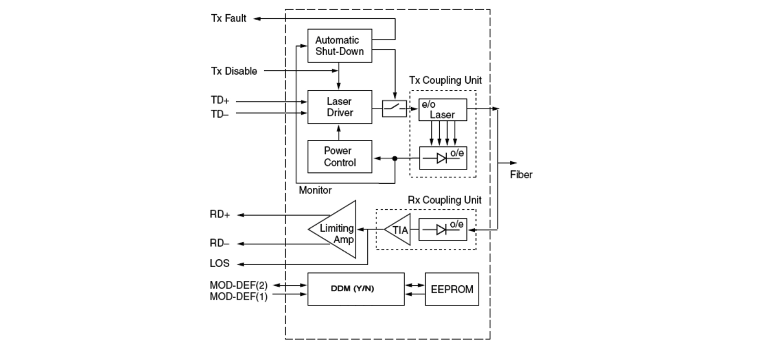
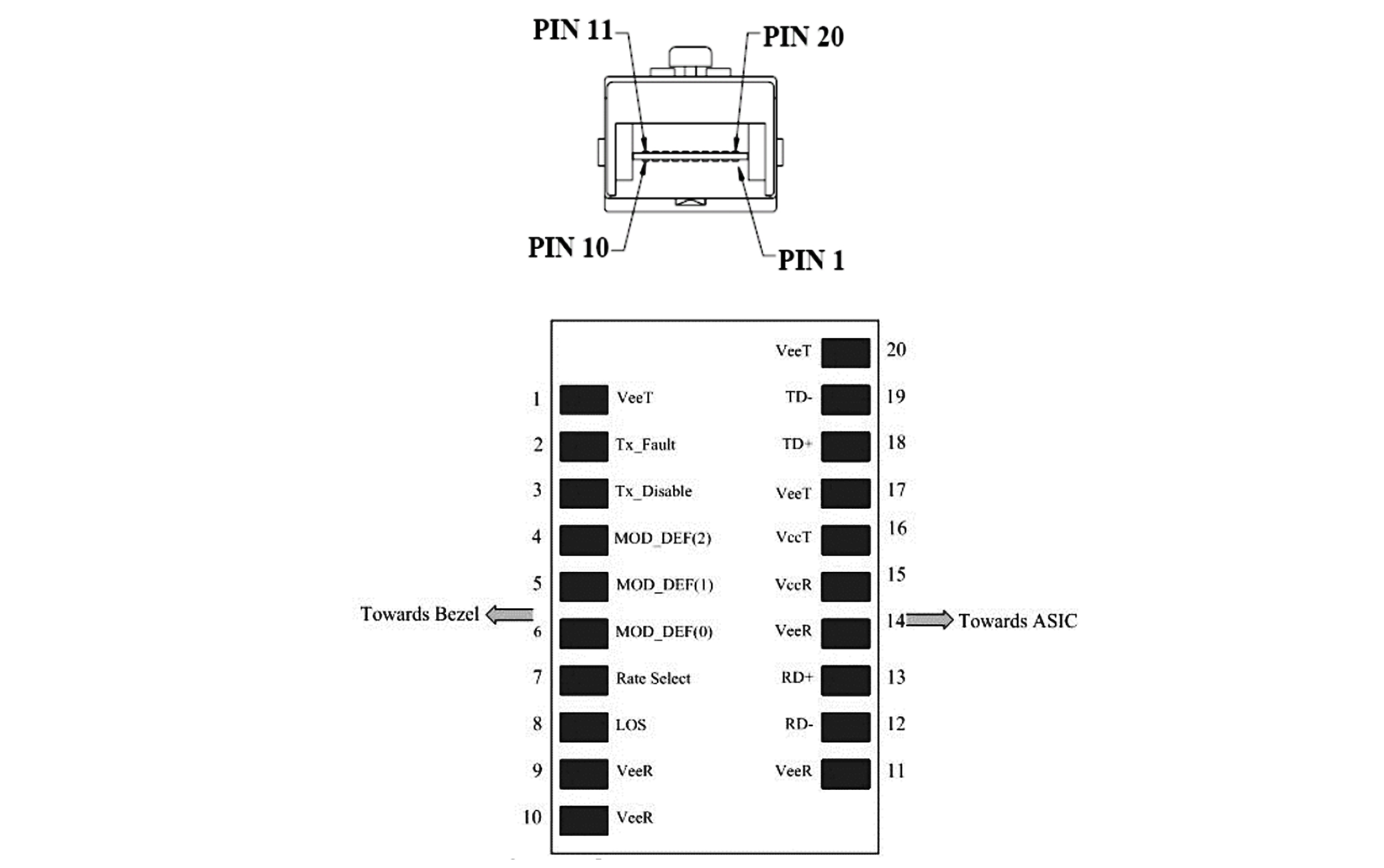
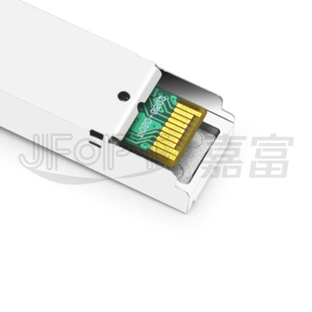
| Pin | Name | Function | Plug Seq. | Notes | |||||
| 1 | VeeT | Transmitter ground | 1 | 5) | |||||
| 2 | TX Fault | Transmitter fault indication | 3 | 1) | |||||
| 3 | TX Disable | Transmitter disable | 3 | 2) Module disables on high or open | |||||
| 4 | MOD-DEF2 | Module definition 2 | 3 | 3) Data line for serial ID. | |||||
| 5 | MOD-DEF1 | Module definition 1 | 3 | 3) Clock line for serial ID. | |||||
| 6 | MOD-DEF0 | Module definition 0 | 3 | 3) Grounded within the module. | |||||
| 7 | Rate Select | Not connect | 3 | Function not available | |||||
| 8 | LOS | Loss of signal | 3 | 4) | |||||
| 9 | VeeR | Receiver ground | 1 | 5) | |||||
| 10 | VeeR | Receiver ground | 1 | 5) | |||||
| 11 | VeeR | Receiver ground | 1 | 5) | |||||
| 12 | RD- | Inv. received data out | 3 | 6) | |||||
| 13 | RD+ | Received data out | 3 | 7) | |||||
| 14 | VeeR | Receiver ground | 1 | 5) | |||||
| 15 | VccR | Receiver power | 2 | 7) 3.3V ± 5% | |||||
| 16 | VccT | Transmitter power | 2 | 7) 3.3V ± 5% | |||||
| 17 | VeeT | Transmitter ground | 1 | 5) | |||||
| 18 | TD+ | Transmit data In | 3 | 8) | |||||
| 19 | TD- | Inv. transmit data In | 3 | 8) | |||||
| 20 | VeeT | Transmitter ground | 1 | 5) | |||||
Notes:
1) TX Fault is an open collector/drain output, which should be pulled up with a 4.7K – 10KΩ resistor on the host board. Pull up voltage between 2.0V and VccT/R+0.3V. When high, output indicates a laser fault of some kinds. Low indicates normal operation. In the low state, the output will be pulled to < 0.8V.
2) TX disable is an input that is used to shutdown the transmitter optical output. It is pulled up within the module with a 4.7K – 10 KΩ resistor. Its states are:
Low (0 – 0.8V): Transmitter on
(>0.8, < 2.0V): Undefined
High (2.0 – 3.465V): Transmitter Disabled
Open: Transmitter Disabled
3) Mod-Def 0,1,2. These are the module definition pins. They should be pulled up with a 4.7K – 10K resistor on the host board. The pull-up voltageshall be VccT or VccR .Mod-Def 0 is grounded by the module to indicate that the module is present.Mod-Def 1 is the clock line of two wire serial interface for serial ID.Mod-Def 2 is the data line of two wire serial interface for serial ID.
4) LOS is an open collector/drain output, which should be pulled up with a 4.7K – 10KΩ resistor. Pull up voltage between 2.0V and VccT/R+0.3V. When high, this output indicates the received optical power is below the worst-case receiver sensitivity (as defined by the standard in use).Low indicates normal operation. In the low state, the output will be pulled to < 0.8V.
5) VeeR and VeeT may be internally connected within the SFP module.
6) RD-/+: These are the differential receiver outputs. They are AC coupled 100Ω differential lines which should be terminated with 100Ω (differential) at the user SERDES. The AC coupling is done inside the module and is thus not required on the host board. The voltage swing on these lines will be between 370 and 2000 mV differential (185 –1000 mV single ended) when properly terminated.
7) VccR and VccT are the receiver and transmitter power supplies. They are defined as 3.3V ±5% at the SFP connector pin. Maximum supply current is 300Ma. Recommended host board power supply filtering is shown below. Inductors with DC resistance of less than 1ohm should be used in order to maintain the required voltage at the SFP input pin with 3.3V supply voltage. When the recommended supply-filtering network is used, hot plugging of the SFP transceiver module will result in an inrush current of no more than 30Ma greater than the steady state value.VccR and VccT may be internally connected within the SFP transceiver module.
8) TD-/+: These are the differential transmitter inputs. They are AC-coupled, differential lines with 100Ω differential termination inside the module.The AC coupling is done inside the module and is thus not required on the host board. The inputs will accept differential swings of 500 – 2400 mV (250 – 1200mV single-ended), though it is recommended that values between 500 and 1200 mV differential (250 – 600mV single-ended) be used for best EMI performance.


 Ann
Ann


