


| Product model | JFTSM-SFP+BD-10-1213-20(ELR)-LC | Manufacturer brand | JFOPT |
| Package type | SFP+ BIDI | Optical connector | LC |
| Max data rate | 11.3Gbps | Channel data rate | 10.3125Gbps |
| Effective transmission distance | 20km | ||
| Wavelength | Tx:1270nm/Rx:1330nm
Tx:1330nm/Rx:1270nm
|
Operating voltage | 3.3V |
| Fiber type | SFP+ BIDI | Core size | 9/125 |
| Transmitter type | 11.3Gbps | Receiver type | IDP |
| TX power | -2~3dBm | Receiver sensitivity | -14dBm |
| Digital optical monitoring(DOM) | YES | Receiver overload | 0.5dBm |
| Power consumption | <1.5W | Protocols | SFF-8431 IEEE 802.3ae 10GBASE-LR IEEE 802.3ae 10GBASE-LW SFF-8472 |
| Operating temperature(Commercial) | 0℃~+70℃ | Storage temperature(Commercial) | -40℃~+85℃ |
| Operating temperature(Industrial) | -40℃~+85℃ | Storage temperature(Industrial) | -40℃~+85℃ |
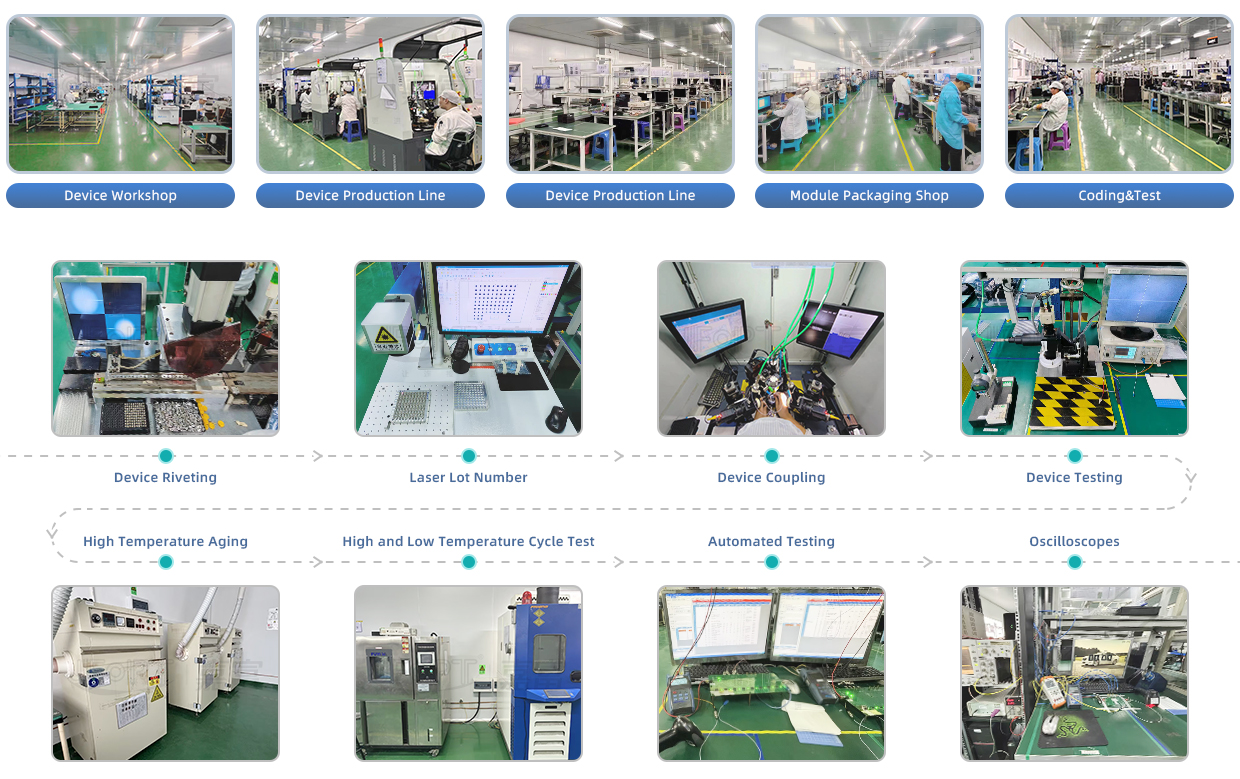
JFOPT continues to invest in optical transceiver production, covering a full range of optical transceiver such as 1*9, SFP, 10G, 25G, 100G, 200G, 400G, 800G GPON/EPON/XG/XGSPON OLT transceiver. At the same time, our company provides TOSA, ROSA, BOSA semi-finished device solutions for the downstream peer. JFOPT's production line has a daily production capacity of 10,000 optical transceivers and 20,000 optical devices. In addition, JFOPT's optical transceiver have industry-leading high temperature resistance and anti-interference capability, and are widely used in computing centers, operators, traffic security, power facilities and other industries.
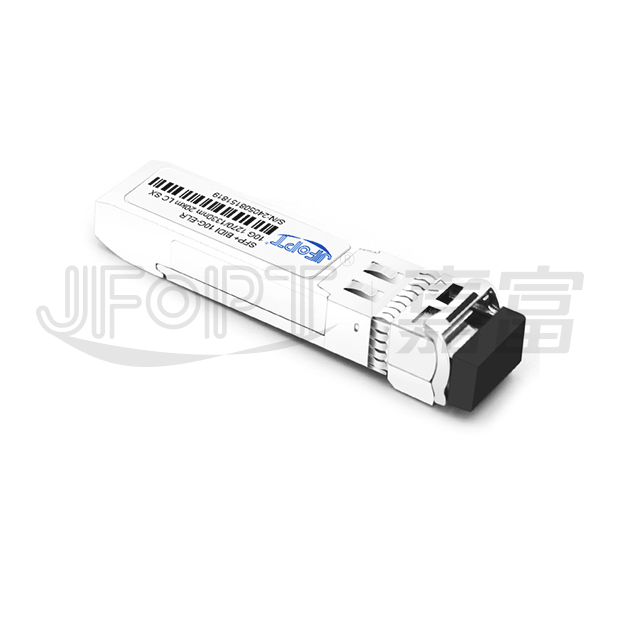
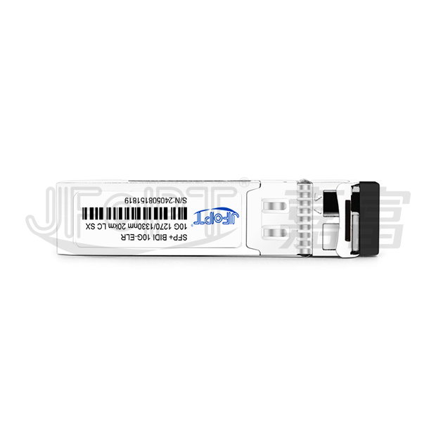
The JFOPT SFP+ BIDI 10G 1270/1330nm 20km ELR LC SX series single-mode transceiver is a compact, pluggable module designed for duplex optical data communication, supporting IEEE 802.3ae 10GBASE-LR/LW standards. It features a 20-pin SFP+ connector for hot-plug capability and is optimized for single-mode fiber, operating at nominal wavelengths of either 1270nm or 1330nm. The transmitter uses a multiple quantum well DFB laser, compliant with Class 1 laser safety standards according to IEC-60825. The receiver integrates an InGaAs detector preamplifier (IDP) within an optical header, paired with a limiting post-amplifier IC for robust signal processing.
| Operating data rate up to 11.3Gbps |
Two types:
A: 1270nm DFB transmitter/ 1330nm receiver
B: 1330nm DFB transmitter/ 1270nm receiver
|
||||||||
| Power budget up to 12dB | Single 3.3V power supply and TTL logic interface | ||||||||
| LC connector interface | Hot pluggable | ||||||||
| Power dissipation < 1.5W |
Operating case temperature
Standard: 0~+70℃
Industrial: -40~+85℃
|
| 10GBASE-LR at 10.3125Gbps | 10GBASE-LW at 9.953Gbps | ||||||||
|
OBSAI rates 6.144 Gb/s, 3.072 Gb/s,
1.536 Gb/s, 0.768Gb/s
|
CPRI rates 10.138Gb/s,9.830Gb/s,7.373Gb/s, 6.144 Gb/s, 4.915Gb/s, 2.458 Gb/s, 1.229 Gb/s,0.614Gb/s | ||||||||
| Other optical links |

| Part No. | Data Rate | Laser | Temp. | Power Budget | Optical Interface | DDMI | ||
| SFP+ BIDI 10G 1270nm 20km ELR LC SX Transceiver | Up to 11.3Gbps | 1270nm DFB | Standard | 12dB | LC | YES | ||
| SFP+ BIDI 10G 1330nm 20km ELR LC SX Transceiver | 1330nm DFB | |||||||
| SFP+ BIDI 10G 1270nm 20km ELR LC SX Transceiver | 1270nm DFB | Industrial | ||||||
| SFP+ BIDI 10G 1330nm 20km ELR LC SX Transceiver | 1330nm DFB | |||||||
| Parameter | Symbol | Min. | Max. | Unit | |||||
| Storage temperature | TS | -40 | +85 | °C | |||||
| Supply voltage | VCC | -0.5 | 3.6 | V | |||||
*Note: Exceeding any one of these values may destroy the device permanently. |
|||||||||
| Parameter | Symbol | Min. | Typical | Max. | Unit | ||||
| Operating case temperature | Tc | 0 | - | +70 | °C | ||||
| -40 | - | 85 | |||||||
| Power supply voltage | Vcc | 3.15 | 3.3 | 3.45 | V | ||||
| Power supply current | Icc | - | - | 430 | mA | ||||
| Surge current | ISurge | - | - | +30 | mA | ||||
| Baud rate | - | 0.6 | 10.3125 | 11.3 | GBaud | ||||
| Parameter | Symbol | Min. | Typ. | Max | Unit | Notes | |||
Transmitter |
|||||||||
| CML inputs(Differential) | Vin | 150 | - | 1200 | mVpp | AC coupled inputs | |||
| Input impedance (Differential) | Zin | 85 | 100 | 115 | ohms | Rin > 100 kohms @ DC | |||
| Tx_DISABLE input voltage - high | - | 2 | - | Vcc+0.3 | V | - | |||
| Tx_DISABLE input voltage - low | - | 0 | - | 0.8 | V | - | |||
| Tx_FAULT output voltage - high | - | 2 | - | Vcc+0.3 | V | Io = 400µA; Host Vcc | |||
| Tx_FAULT output voltage - low | - | 0 | - | 0.5 | V | Io = -4.0mA | |||
Receiver |
|||||||||
| CML outputs (Differential) | Vout | 350 | - | 700 | mVpp | AC coupled outputs | |||
| Output impedance (Differential) | Zout | 85 | 100 | 115 | ohms | - | |||
| Rx_LOS output voltage - high | - | 2 | - | Vcc+0.3 | V | lo = 400µA; Host Vcc | |||
| Rx_LOS output voltage - low | - | 0 |
-
|
0.8
|
V | lo = -4.0mA | |||
| MOD_DEF ( 2:0 ) | VoH | 2.5 | - | - | V | With serial ID | |||
| VoL | 0 | - | 0.5 | V | |||||
1270nm DFB & PIN/TIA |
|||||||||
| Parameter | Symbol | Min. | Typical | Max. | Unit | ||||
| Power budget | - | 12 | - | - | dB | ||||
| Data rate | - | 0.6 | 10.3125 | 11.3 | Gbps | ||||
Transmitter |
|||||||||
| Centre wavelength | λC | 1260 | 1270 | 1280 | nm | ||||
| Spectral width (-20dB) | Δλ | - | - | 1 | nm | ||||
| Side mode suppression ratio | SMSR | 30 | - | - | dB | ||||
| Average output power | Pout, AVG | -2 | - | 3 | dBm | ||||
| Extinction ratio | ER | 3.5 | - | - | ms | ||||
| Average power of OFF transmitter | - | - | - | -30 | dBm | ||||
| Relative intensity noise | RIN | - | - | -128 | dB/Hz | ||||
| TX disable assert time | t_off | - | - | 10 | us | ||||
Receiver |
|||||||||
| Centre wavelength | λc | 1320 | - | 1340 | nm | ||||
| Sensitivity | PIN | - | - | -14 | dBm | ||||
| Receiver overload | PMAX | 0.5 | - | - | dBm | ||||
| LOS de-assert | LOSD | - | - | -18 | dBm | ||||
| LOS assert | LOSA | -30 | - | - | dBm | ||||
1330nm DFB & PIN/TIA |
|||||||||
| Parameter | Symbol | Min. | Typical | Max. | Unit | ||||
| Power budget | - | 12 | - | - | dB | ||||
| Data rate | - | 0.6 | 10.3125 | 11.3 | Gbps | ||||
Transmitter |
|||||||||
| Centre wavelength | λC | 1320 | 1330 | 1340 | nm | ||||
| Spectral width (-20dB) | Δλ | - | - | 1 | nm | ||||
| Side mode suppression ratio | SMSR | 30 | - | - | dB | ||||
| Average output power | Pout, AVG | -2 | - | 3 | dBm | ||||
| Extinction ratio | ER | 3.5 | - | - | dB | ||||
| Average power of OFF transmitter | - | - | - | -30 | dBm | ||||
| Relative intensity noise | RIN | - | - | -128 | dB/Hz | ||||
| TX disable assert time | t_off | - | - | 10 | us | ||||
Receiver |
|||||||||
| Centre wavelength | λc | 1260 | - | 1280 | nm | ||||
| Sensitivity | PIN | - | - | -14 | dBm | ||||
| Receiver overload | PMAX | - | - | - | dBm | ||||
| LOS de-assert | LOSD | - | - | -18 | dBm | ||||
| LOS assert | LOSA | -30 | - | - | dBm | ||||
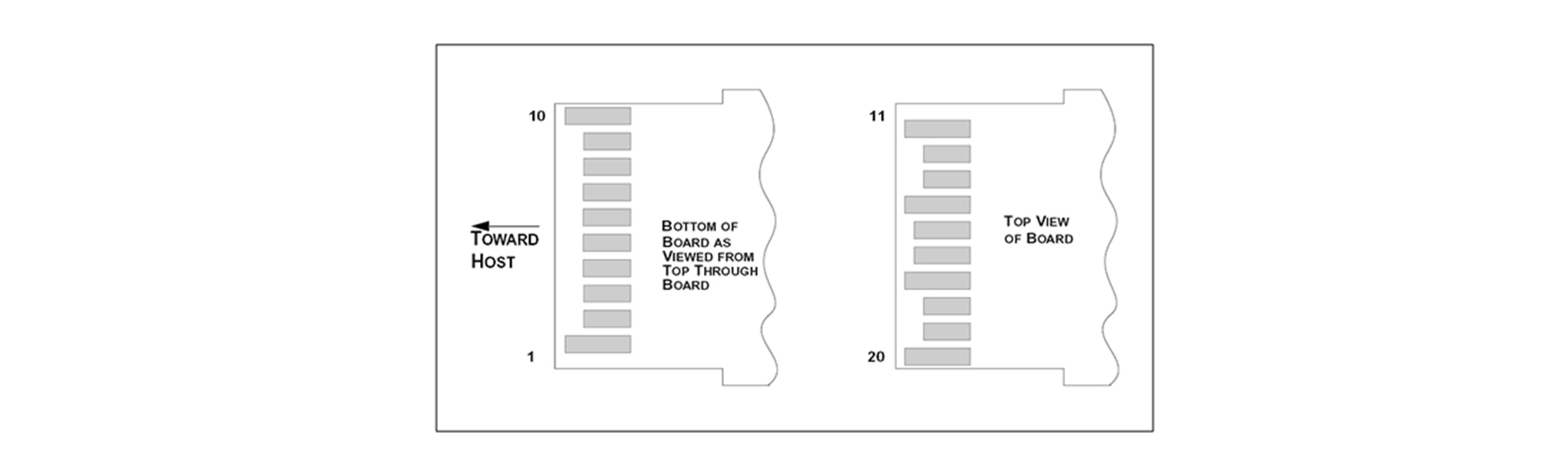

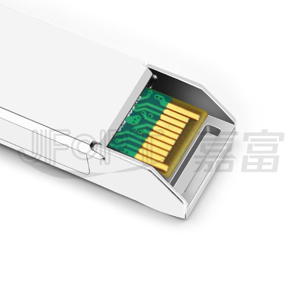
| Pin Num. | Name | Function | Plug Seq. | Notes | ||||
| 1 | VeeT | Transmitter ground | 1 | Note 5 | ||||
| 2 | TX fault | Transmitter fault indication | 3 | Note 1 | ||||
| 3 | TX disable | Transmitter disable | 3 | Note 2, module disables on high or open | ||||
| 4 | SDA | Module definition 2 | 3 | 2-Wire serial interface data line. | ||||
| 5 | SCL | Module definition 1 | 3 | 2-Wire serial interface clock. | ||||
| 6 | MOD_ABS | Module definition 0 | 3 | Note 3 | ||||
| 7 | RS0 | RX Rate select(LVTTL). | 3 | No function implement | ||||
| 8 | LOS | Loss of signal | 3 | Note 4 | ||||
| 9 | RS1 | TX Rate select(LVTTL). | 1 | No function implement | ||||
| 10 | VeeR | Receiver ground | 1 | Note 5 | ||||
| 11 | VeeR | Receiver ground | 1 | Note 5 | ||||
| 12 | RD- | Inv. received data out | 3 | Note 6 | ||||
| 13 | RD+ | Received data out | 3 | Note 6 | ||||
| 14 | VeeR | Receiver ground | 1 | Note 5 | ||||
| 15 | VccR | Receiver power | 2 | 3.3V ± 5%, Note 7 | ||||
| 16 | VccT | Transmitter power | 2 | 3.3V ± 5%, Note 7 | ||||
| 17 | VeeT | Transmitter ground | 1 | Note 5 | ||||
| 18 | TD+ | Transmit data in | 3 | Note 8 | ||||
| 19 | TD- | Inv. transmit data in | 3 | Note 8 | ||||
| 20 | VeeT | Transmitter ground | 1 | Note 5 | ||||
Notes: 1) TX Fault is an open collector/drain output, which should be pulled up with a 4.7K – 10KΩ resistor on the host board. Pull up voltage between 2.0V and VccT/R+0.3V. When high, output indicates a laser fault of some kind. Low indicates normal operation. In the low state, the output will be pulled to < 0.8V. 2) TX disable is an input that is used to shut down the transmitter optical output. It is pulled up within the module with a 4.7K – 10 KΩ resistor. Its states are: Low (0 – 0.8V): Transmitter on (>0.8, < 2.0V): Undefined High (2.0 – 3.465V): Transmitter Disabled Open: Transmitter Disabled 3) Module Absent, connected to VeeT or VeeR in the module. 4) LOS (Loss of Signal) is an open collector/drain output, which should be pulled up with a 4.7K – 10KΩ resistor. Pull up voltage between 2.0V and VccT/R+0.3V. When high, this output indicates the received optical power is below the worst-case receiver sensitivity (as defined by the standard in use). Low indicates normal operation. In the low state, the output will be pulled to < 0.8V. 5) The module signal ground contacts, VeeR and VeeT, should be isolated from the module case. 6) RD-/+: These are the differential receiver outputs. They are AC coupled 100Ω differential lines which should be terminated with 100Ω (differential) at the user SERDES. The AC coupling is done inside the module and is thus not required on the host board. The voltage swing on these lines will be between 350 and 700 mV differential (175 –350 mV single ended) when properly terminated. 7) VccR and VccT are the receiver and transmitter power supplies. They are defined as 3.3V ±5% at the SFP+ connector pin. Maximum supply current is 430mA. Recommended host board power supply filtering is shown below. Inductors with DC resistance of less than 1 ohm should be used in order to maintain the required voltage at the SFP+ input pin with 3.3V supply voltage. When the recommended supply-filtering network is used, hot plugging of the SFP+ transceiver module will result in an inrush current of no more than 30mA greater than the steady state value. VccR and VccT may be internally connected within the SFP+ transceiver module. 8) TD-/+: These are the differential transmitter inputs. They are AC-coupled, differential lines with 100Ω differential termination inside the module. The AC coupling is done inside the module and is thus not required on the host board. The inputs will accept differential swings of 150 – 1200 mV (75 – 600mV single-ended). |
||||||||


 Ann
Ann


