


| Product model | JFTSM-SFP+10-CW1216-LR-LCD | Manufacturer brand | JFOPT |
| Package type | SFP+ | Optical connector | LC Duplex |
| Max data rate | 11.3Gbps | Channel data rate | 10.31Gbps |
| Powerbudget | >10dB,>14dB | ||
| Wavelength | 1270nm to 1610nm | Operating voltage | 3.3V |
| Fiber type | SMF | Core size | 9/125 |
| Transmitter type | CWDM DFB | Receiver type | IDP |
| TX power | -1~4dBm | Receiver sensitivity | -15dBm |
| Digital optical monitoring(DOM) | YES | Receiver overload | 0.5dBm |
| Power consumption | <1W | Protocols | SFP+ MSA
SFF-8431
SFF-8472
|
| Operating temperature(Commercial) | 0℃~+70℃ | Storage temperature(Commercial) | -40℃~+85℃ |
| Operating temperature(Extended) | -20℃~+75℃ | Storage temperature(Industrial) | -40℃~+85℃ |
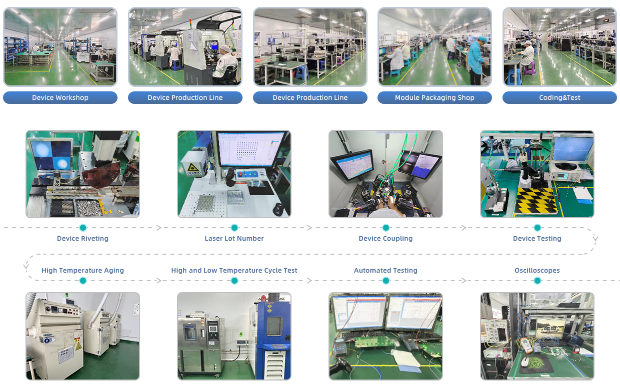
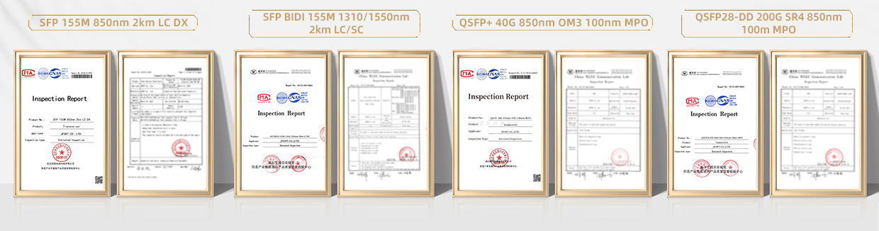
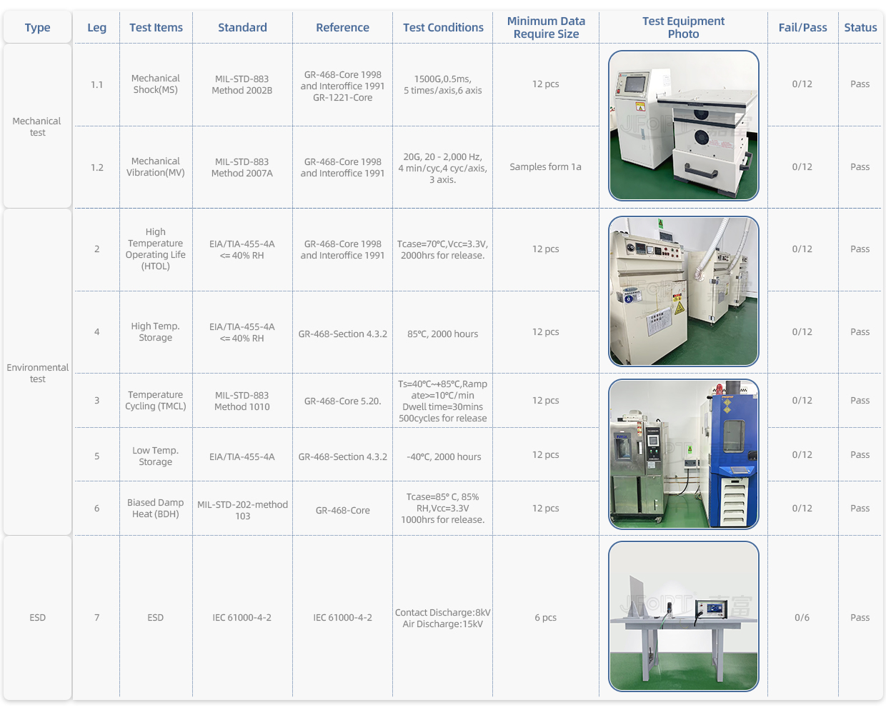
JFOPT continues to invest in optical transceiver production, covering a full range of optical transceiver such as 1*9, SFP, 10G, 25G, 100G, 200G, 400G, 800G GPON/EPON/XG/XGSPON OLT transceiver. At the same time, our company provides TOSA, ROSA, BOSA semi-finished device solutions for the downstream peer. JFOPT's production line has a daily production capacity of 10,000 optical transceivers and 20,000 optical devices. In addition, JFOPT's optical transceiver have industry-leading high temperature resistance and anti-interference capability, and are widely used in computing centers, operators, traffic security, power facilities and other industries.
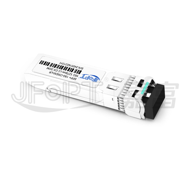
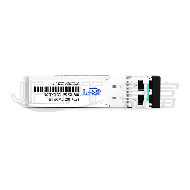
The JFOPT SFP+ 10G CWDM (1270-1610nm) LR LC DX series optical transceiver is specifically designed for fiber communication applications such as 10G Ethernet (10GBASE-LR/LW). Fully compliant with the SFP+ MSA specification SFF-8431, this module supports single-mode fiber operation at CWDM wavelengths, offering multiple center wavelengths ranging from 1270nm to 1610nm, with 20nm increments.Featuring an SFP+ connector for hot-plug capability, the module requires a single 3.3V power supply. Key functions include TX_DIS for disabling the optical output via LVTTL logic high input and RX_LOS to indicate the loss of an input optical signal. Additionally, it supports digital diagnostic monitoring via a 2-wire serial interface as per the SFF-8472 specification.

| Up to 11.3Gb/s bit rate | Hot-pluggable SFP+ footprint | ||||||||
| 18-Wavelength CWDM DFB transmitter from 1270nm to 1610nm, with step 20nm | 10dB/14dB power budget at least | ||||||||
| Duplex LC connector | Power dissipation < 1.2W | ||||||||
| Case operation temperature range: Standard: -5°C to 70°C Extended: -20°C to 75°C |
Build-in digital diagnostic functions |
| 10GBASE-LR/LW/ER/EW 10G ethernet | 10GBASE-ER at 10.31Gbps | ||||||||
| 10GBASE-LW/EW at 9.95Gbps | OBSAI rates 6.144 Gb/s, 3.072 Gb/s, 1.536 Gb/s, 0.768Gb/s | ||||||||
| CPRI Rates 10.138Gb/s, 9.830 Gb/s,7.373Gb/s, 6.144 Gb/s,4.915 Gb/s, 2.458 Gb/s, 1.229 Gb/s, 0.614Gb/s | Other optical links |

| Part No. | Version | Data Rate | Laser | Fiber | Power Budget | Temp. | Interface | ||
| JFTSM-SFP+10-CW1216-LR-LCD-10X | Standard | Up to 11.3Gb/s | CWDM DFB | SMF | >10dB | -5°C to 70°C | LC | ||
| Extended | -20°C to 75°C | ||||||||
| JFTSM-SFP+10-CW1216-LR-LCD-14X | Standard | 0.614Gbps to 11.3Gbps | >14dB | -5~70°C | |||||
| *Note: X refers to CWDM Wavelength range 1270nm to 1610nm, X=A~R, denotes 1270nm to 1610nm. | |||||||||
| Band | Nomenclature | Wavelength(nm) | |||||||
| Min. | Typ. | Max. | |||||||
| O-band Original | A | 1264 | 1270 | 1277.5 | |||||
| B | 1284 | 1290 | 1297.5 | ||||||
| C | 1304 | 1310 | 1317.5 | ||||||
| D | 1324 | 1330 | 1337.5 | ||||||
| E | 1344 | 1350 | 1357.5 | ||||||
| E-band Extended | F | 1364 | 1370 | 1377.5 | |||||
| G | 1384 | 1390 | 1397.5 | ||||||
| H | 1404 | 1410 | 1417.5 | ||||||
| I | 1424 | 1430 | 1437.5 | ||||||
| J | 1444 | 1450 | 1457.5 | ||||||
| S-band Short Wavelength | K | 1464 | 1470 | 1477.5 | |||||
| L | 1484 | 1490 | 1497.5 | ||||||
| M | 1504 | 1510 | 1517.5 | ||||||
| N | 1524 | 1530 | 1537.5 | ||||||
| C-band Conventional | O | 1544 | 1550 | 1557.5 | |||||
| L-band Long Wavelength | P | 1564 | 1570 | 1577.5 | |||||
| Q | 1584 | 1590 | 1597.5 | ||||||
| R | 1604 | 1610 | 1617.5 | ||||||
| CWDM*: 18 Wavelengths from 1270nm to 1610nm, each step 20nm. |
|||||||||
| Parameter | Symbol | Min. | Typical | Max. | Unit | ||||
| Maximum supply voltage | Vcc | -0.5 | - | 4.0 | V | ||||
| Storage temperature | Ts | -40 | - | 85 | °C | ||||
| Parameter | Symbol | Min. | Typical | Max. | Unit | ||||
| Operating case temperature range | Tc | -5 | - | +70 | ℃ | ||||
| Supply voltage | Vcc | 3.13 | 3.3 | 3.45 | V | ||||
| Supply current | Icc | - | - | 350 | mA | ||||
| Data rate | - | 0.614 | - | 11.3 | Gbps | ||||
| Parameter | Symbol | Min. | Typ. | Max. | Unit | Notes | |||
Transmitter |
|||||||||
| CML inputs(Differential) | Vin | 150 | - | 1200 | mVpp | 1 | |||
| Input impedance (Differential) | Zin | 85 | 100 | 115 | ohm | - | |||
| Tx_DISABLE input voltage - high | - | 2 | - | Vcc+0.3 | V | - | |||
| Tx_DISABLE input voltage -low | - | 0 | - | 0.8 | V | - | |||
| Tx_FAULT output voltage - high | - | 2 | - | Vcc+0.3 | V | - | |||
| Tx_FAULT output voltage - low | - | 0 | - | 0.8 | V | - | |||
Receiver |
|||||||||
| CML outputs (Differential) | Vout | 350 | - | 700 | mVp-p | 1 | |||
| Output impedance (Differential) | Zout | 85 | 100 | 115 | ohm | - | |||
| Rx_LOS output voltage - high | - | 2 | - | Vcc+0.3 | V | - | |||
| Rx_LOS output voltage - low | - | 0 | - | 0.8 | V | - | |||
| MOD_DEF ( 0:2 ) | VoH | 2.5 | - | - | V | 2 | |||
| VoL | 0 | - | 0.5 | V | |||||
*Notes: 1. After internal AC coupling. 2. Reference the SFF-8472 MSA. |
|||||||||
| Parameter | Symbol | Unit | Note | JFTSM-SFP+10-CW1216-LR-LCD-10X | JFTSM-SFP+10-CW1216-LR-LCD-14X | |||||
| Min. | Typical | Max. | Min. | Typical | Max. | |||||
Transmitter |
||||||||||
| Output opt. pwr: 9/125 SMF | Pout | dBm | 1 | -5 | - | 0 | -1 | - | 4 | |
| Optical extinction ratio | ER | dB | - | 3.5 | - | - | 3.5 | - | - | |
| Optical wavelength | λ | nm | 2 | λc–6 | λc | λc+7.5 | λc–6 | λc | λc+7.5 | |
| -20dB spectrum width | Δλ | nm | - | - | - | 1 | - | - | 1 | |
| Side mode suppression ratio | SMSR | dB | - | 30 | - | - | 30 | - | - | |
| Transmitterand dispersion penalty | TDP | dB | - | - | - | 2 | - | - | 2 | |
| Average launch power of OFF transmitter | POFF | dBm | - | - | - | -30 | - | - | -30 | |
Receiver |
||||||||||
| Receiver sensitivity @ 10.7Gb/s | Pmin | dBm | 3 | - | - | -15 | - | - | -15 | |
| Maximum input power | Pmax | dBm | - | +0.5 | - | - | +0.5 | - | - | |
| Optical center wavelength | λ | nm | - | 1260 | - | 1620 | 1260 | - | 1620 | |
| Receiver reflectance | Rrf | dB | - | - | - | -27 | - | - | -27 | |
| LOS de-assert | LOSD | dBm | - | - | - | -16 | - | - | -16 | |
| LOS assert | LOSA | dBm | - | -28 | - | - | -28 | - | - | |
| LOS hysteresis | - | dB | - | 1 | - | - | 1 | - | - | |
*Notes: 1. Output power is coupled into a 9/125μm SMF. 2. ITU-T G.694.2 CWDM wavelength from 1270nm to 1610nm, each step 20nm. 3. Average received power; BER less than 1E-12 and PRBS 231-1 test pattern. |
||||||||||
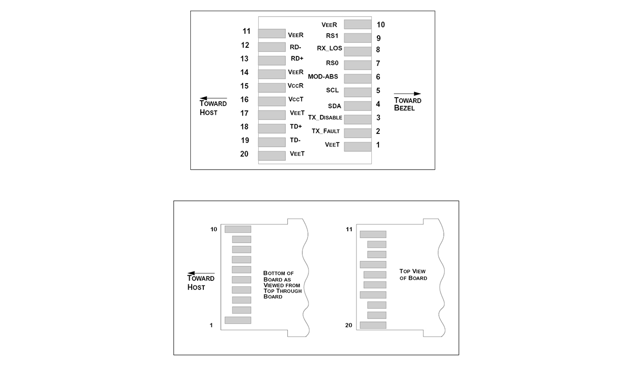
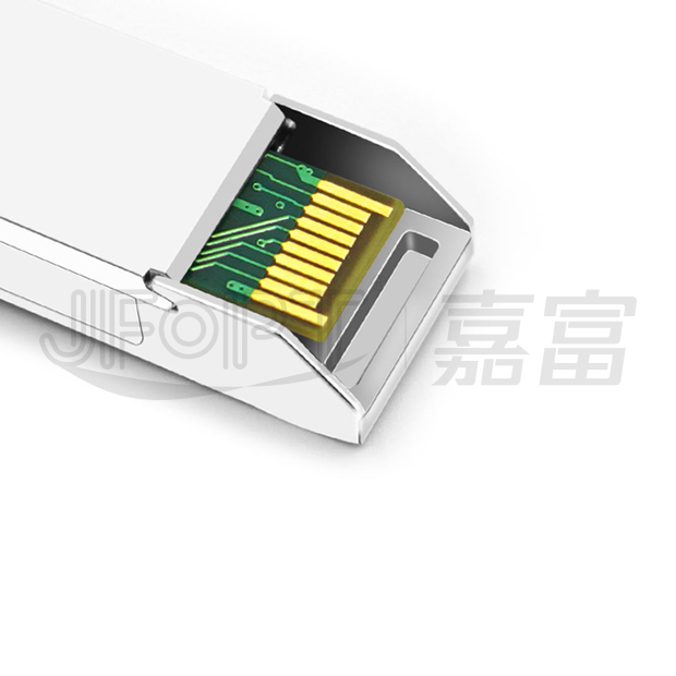
| Pin Num. | Name | Function | Plug Seq. | Notes | |||||
| 1 | VeeT | Transmitter ground | 1 | Note 5 | |||||
| 2 | TX fault | Transmitter fault indication | 3 | Note 1 | |||||
| 3 | TX disable | Transmitter disable | 3 | Note 2, module disables on high or open | |||||
| 4 | SDA | Module definition 2 | 3 | Data line for serial ID | |||||
| 5 | SCL | Module definition 1 | 3 | Clock line for serial ID. | |||||
| 6 | MOD_ABS | Module definition 0 | 3 | Note 3 | |||||
| 7 | RS0 | RX rate select(LVTTL). | 3 | No function implement.. | |||||
| 8 | LOS | Loss of signal | 3 | Note 4 | |||||
| 9 | RS1 | TX rate select(LVTTL). | 1 | No function implement.. | |||||
| 10 | VeeR | Receiver ground | 1 | Note 5 | |||||
| 11 | VeeR | Receiver ground | 1 | Note 5 | |||||
| 12 | RD- | Inv. received data out |
3
|
Note 6 | |||||
| 13 | RD+ | Received data out | 3 | Note 6 | |||||
| 14 | VeeR | Receiver ground | 1 | Note 5 | |||||
| 15 | VccR | Receiver power | 2 | 3.3V ± 5%, Note 7 | |||||
| 16 | VccT | Transmitter power | 2 | 3.3V ± 5%, Note 7 | |||||
| 17 | VeeT | Transmitter ground | 1 | Note 5 | |||||
| 18 | TD+ | Transmit data in | 3 | Note 8 | |||||
| 19 | TD- | Inv. transmit data in | 3 | Note 8 | |||||
| 20 | VeeT | Transmitter ground | 1 | Note 5 | |||||
Notes:
1) . TX Fault is an open collector/drain output, which should be pulled up with a 4.7K - 10KΩ resistor on the host board. Pull up voltage between 2.0V and VccT, R+0.3V. When high,output indicates a laser fault of some kind. Low indicates normal operation. In the low state, the output will be pulled to < 0.8V
2) . TX disable is an input that is used to shut down the transmitter optical output. It is pulled up within the module with a 4.7-10KΩ resistor. Its states are: Low (0 - 0.8V): Transmitter on(>0.8, < 2.0V): Undefined High (2.0 - 3.465V):Transmitter Disabled Open: Transmitter Disabled
3)Module absent, connected to VEET or VEER in the module
4) LOS (Loss of Signal) is an open collector/drain output, which should be pulled up with a 4.7K–10KΩ resistor. Pull up voltage between 2.0V and VccT, R+0.3V. When high, this output indicates the received optical power is below the worst-case receiver sensitivity (as defined by the standard in use). Low indicates normal operation. In the low state, the output will be pulled to < 0.8V.
5) VeeR and VeeT may be internally connected within the SFP+ module.
6) RD-/+: These are the differential receiver outputs. They are AC coupled 100Ω differential lines which should be terminated with100Ω(differential) at the user SERDES. The AC coupling is done inside the module and is thus not required on the host board.
7) VccR and VccT are the receiver and transmitter power supplies. They are defined as 3.3V ±5% at the SFP+ connector pin. Maximum supply current is 300mA. Inductors with DC resistance of less than 1 ohm should be used in order to maintain the required voltage at the SFP+ input pin with 3.3V supply voltage. When the recommended supply-filtering network is used, hot plugging of the SFP+ transceiver module will result in an inrush current of no more than 30mA greater than the steady state value. VccR and VccT may be internall connected within the SFP+ transceiver module
8) . TD-/+: These are the differential transmitter inputs. They are AC-coupled, differential lines with 100 differential termination inside the module. The AC coupling is done inside the module and is thus not required on the host board.


 Ann
Ann


