


|
Product model
|
JFTSM-SFP+10-50DW-40(ER)-LCD
|
Manufacturer brand
|
JFOPT
|
|
Package type
|
SFP+
|
Optical connector
|
LC Duplex
|
|
Max data rate
|
11.3Gbps
|
Channel data rate
|
10.3125Gbps
|
|
Effective transmission distance
|
40km
|
||
|
Wavelength
|
1529.16~1567.13nm(Tunable)
|
Operating voltage
|
3.3V
|
|
Fiber type
|
SMF
|
Core size
|
9/125
|
|
Transmitter type
|
Monolithic MZM Tunable TOSA
|
Receiver type
|
PIN
|
|
TX power
|
-1~3dBm,-1~4dBm
|
Receiver sensitivity
|
-16dBm
|
|
Digital optical monitoring(DOM)
|
YES
|
Receiver overload
|
-1dBm
|
|
Power consumption
|
C<2.1W,I<2.5W
|
Protocols
|
SFF-8431
SFF-8472
SFF-8690
IEEE 802.3ae CL 52
|
|
Operating temperature(Commercial)
|
0℃~+70℃
|
Storage temperature(Commercial)
|
-40℃~+85℃
|
|
Operating temperature(Industrial)
|
-40℃~+85℃
|
Storage temperature(Industrial)
|
-40℃~+85℃
|
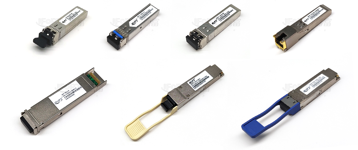
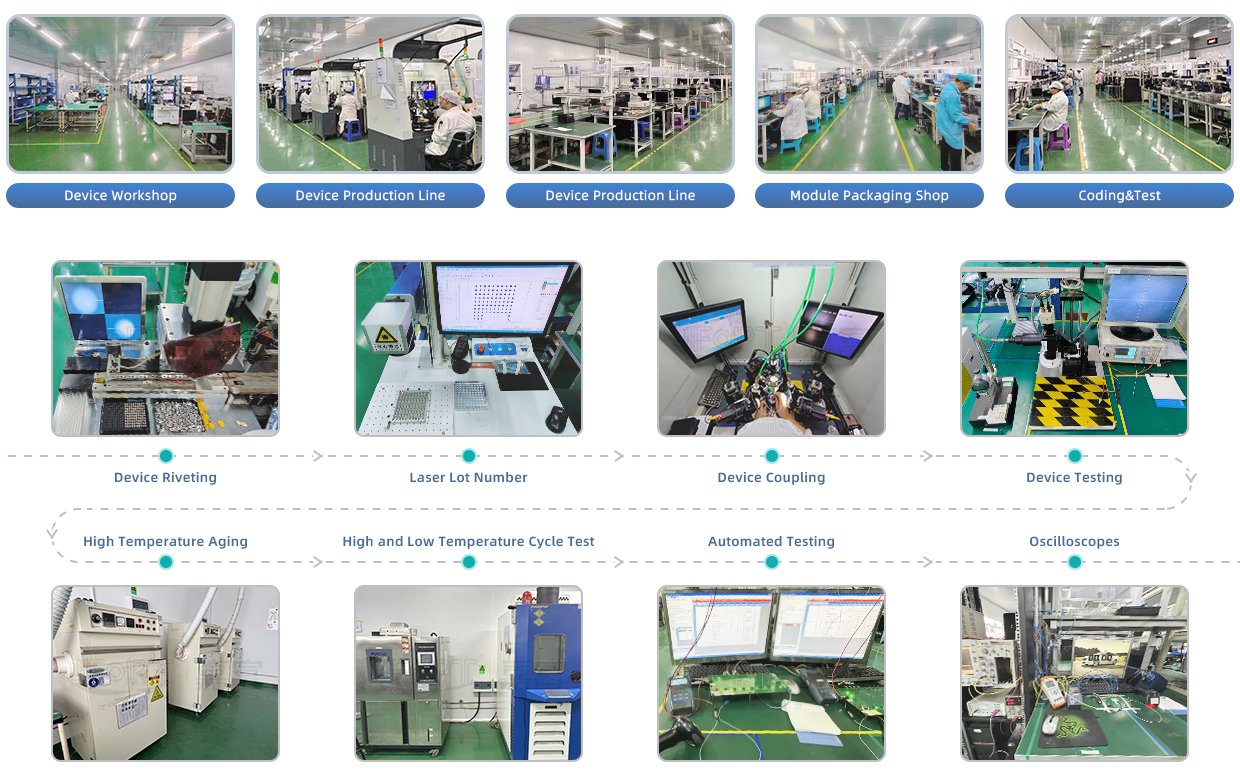
JFOPT continues to invest in optical transceiver production, covering a full range of optical transceiver such as 1*9, SFP, 10G, 25G, 100G, 200G, 400G, 800G GPON/EPON/XG/XGSPON OLT transceiver. At the same time, our company provides TOSA, ROSA, BOSA semi-finished device solutions for the downstream peer. JFOPT's production line has a daily production capacity of 10,000 optical transceivers and 20,000 optical devices. In addition, JFOPT's optical transceiver have industry-leading high temperature resistance and anti-interference capability, and are widely used in computing centers, operators, traffic security, power facilities and other industries.
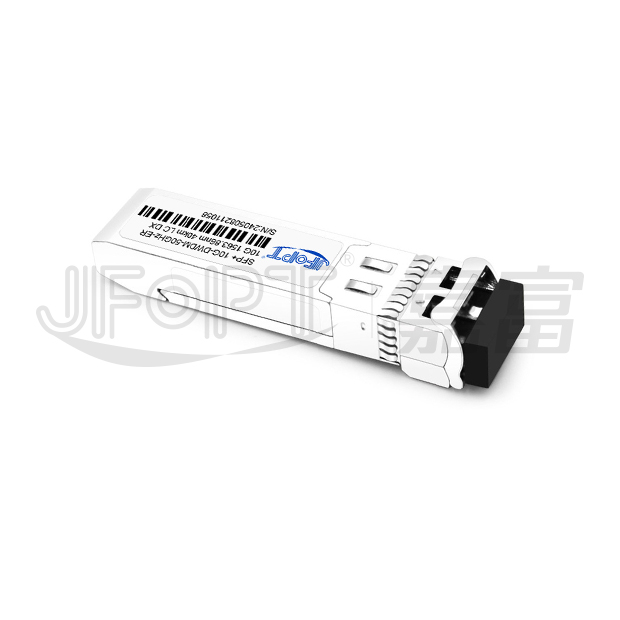
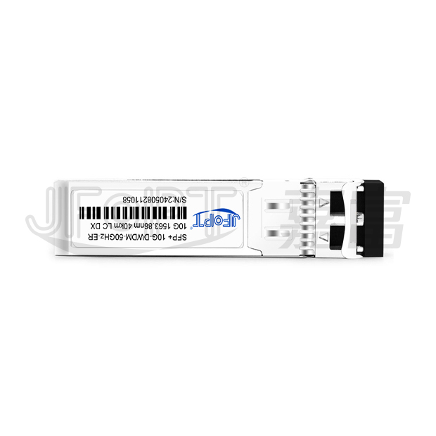
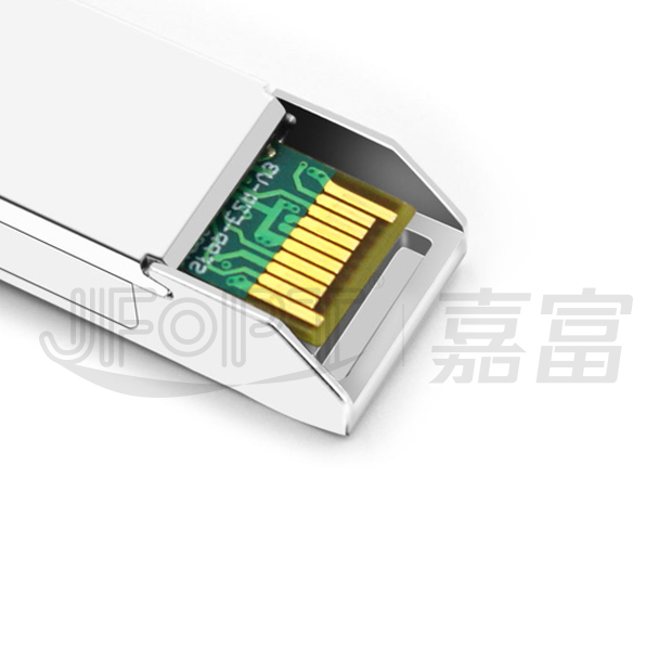
The JFOPT SFP+ 10G 50GHz DWDM 40km ER LC DX is a high performance, cost effective module supporting multi rate 9.95Gbps to 11.3Gbps with CDR, 8.5Gbps bypass CDR, and transmission distance up to 40km on SM fiber; the transceiver consists of two sections: transmitter incorporating a laser driver and TTOSA, and receiver with PIN integrated transimpedance preamplifier (TIA); this hot-pluggable module connects via 20-pin connector, featuring high-speed electrical interface based on low voltage logic with nominal 100ohms differential impedance and AC coupling; optical output is disabled by LVTTL high-level TX_DIS input, while Tx_Fault indicates laser-related faults and RX_LOS signals receiver input loss; its serial EEPROM enables monitoring/configuration access via 2-wire SFP management interface using single address A0h, with memory map divided into lower area (storing basic DD data) and upper area housing specific data in high memory tables.
| Up to 40km transmission on SMF | Support multi rate 9.95Gbps to 11.3Gbpswith CDR, 8.5Gbps bypass CDR | ||||||||
| Monolithic MZM tunable TOSA | PIN receiver | ||||||||
| 50GHz ITU-based channel spacing (C-Band) with a wavelength locker | SFI electrical interface | ||||||||
| 2-wire interface for integrated digital diagnostic monitoring | Hot pluggable | ||||||||
| Very low EMI and excellent ESD protection | +3.3V power supply power consumption less than 2.1W | ||||||||
| Operating case temperature: 0~75°C | SFP+ MSA package with duplex LC conn |
| DWDM 10Gb/s SONET/SDH | DWDM 10Gb/s ethernet & 10Gb/s fibre channel | ||||||||
| DWDM 10Gb/s SONET/SDH w/FEC | DWDM 10Gb/s ethernet & 10Gb/s fibre channel w/FEC |

| Parameter | Symbol | Min. | Max. | Unit | Notes | ||||
| Storage temperature | Ts | -40 | 85.0 | ℃ | - | ||||
| Power supply voltage | Vcc3 | 0 | 3.63 | V | - | ||||
| Relative humidity(noncondensation) | RH | 5 | +85 | % | Note1 | ||||
| Damage threshold | Pmax | - | - | dBm | - | ||||
| Parameter | Symbol | Min. | Typ. | Max. | Unit | Notes | |||
| Operating case temperature | Tc | 0 | 25 | 75 | °C | - | |||
| Supply voltage | Vcc | 3.13 | 3.3 | 3.47 | V | - | |||
| Power supply current | Pd | - | - | 670 | mA | - | |||
| Data rate | - | 8.5 | 10.3125 | 11.3 | Gbps | - | |||
| Transmission distance | - | - | - | 40 | km | - | |||
| Parameter | Symbol | Min. | Typical | Max | Unit | Note | |||
| Data rate | DR | 8.5 | 10.3125 | 11.3 | Gbps | - | |||
| Center wavelength | CW | 191.3 | - | 196.05 | THz | - | |||
| Wavelength range | λC | 1529.16 | - | 1567.13 | nm | - | |||
| Center frequqncy variation | CFV | 0 | - | +/-2.5 | GHz | - | |||
| -20dB spectral width | Δλ20 | - | - | 0.3 | nm | - | |||
| Side mode suppression ratio | SMSR | 30 | - | - | nm | - | |||
| Laser off power | Poff | - | - | -30 | dBm | - | |||
| Transmitter reflectance | TR | - | - | -12 | dB | - | |||
| Average optical power | PO | -1 | 0.5 | 3 | dBm | - | |||
| Extinction ratio | ER | 8.2 | - | - | dB | - | |||
| Cross point of eye | CP | 40% | - | 0.52 | - | - | |||
| Transmitter dispersion renalty | TDP | - | - | 3 | dB | - | |||
| Transmitter dispersion tolerance(CD window with 2dB OSNR penalty) | TDT | -700 | - | 700 | km ps/nm | - | |||
| Relative intensity noise | RIN12OMA | - | - | -128 | dB/Hz | - | |||
| Optical eye mask | EMM | 5 | - | - | - | - | |||
| Tx Input diff voltage | VI | 200 | - | 850 | mV | - | |||
| Parameter | Symbol | Min. | Typical | Max. | Unit | Note | |||
| Data rate | DR | 8.5 | 10.3125 | 11.3 | Gbps | - | |||
| Center wavelength | CW | 1260 | - | 1600 | nm | - | |||
| Sensitivity @(BER=1E-12, PRBS 2^31-1, NRZ, 9.95Gbps~10.7Gbps data rate |
Psen | 1529.16 | - | -16(EOL) | dBm | - | |||
| Sensitivity @(BER=2.0E-03, PRBS 2^31-1,NRZ,11.3Gbps data rate, dispersion 800ps/nm, at room temperature and OSNR >31dB) | Psen | - | - | -19 (EOL) | dBm | - | |||
| B2B OSNR Tolerance BOL @ 2E-3 Test condition: A:optical filter type and bandwidth:flattop filter-3dB bandwidth 84 GHz, OSA res 0.1nm for noise bandwidth. B: Input optical power range: 0~-14dBm C:9.9Gbps~11.3Gbps data rate range D:-5~70℃ E:Under the optimal threshold or 50% threshold |
- | - | - | 13.5 | dB | - | |||
| B2B OSNR Tolerance BOL @ 2E-3 Test condition: A:optical filter type and bandwidth:flattop filter -3dB bandwidth 84 GHz, OSA res 0.1nm for noise bandwidth. B: Input optical power range: 0~-14dBm C:9.9Gbps~11.3Gbps data rate range D:-5~70℃ E:Under the optimal threshold or 50% threshold |
- | - | - | 14.0 | dB | - | |||
| Saturation power(EOL) | SP | -1 | - | - | dBm | - | |||
| Input optical power(no | IOP | 4 | - | - | dBm | - | |||
| Parameter | Symbol | Min. | Typical | Max | Units | Notes | |||
| Temperature monitor absolute error | DMI_Temp | -3 | - | 3 | ℃ | Over operating temperature | |||
| Supplyvoltage monito rabsolute error | DMI_Vcc | -3% | - | 3% | V | Over operating voltage | |||
| Bias current monitor absolute error | DMI_Ibias | -10% | - | 10% | mA | - | |||
| Lase rpower monitor absolute error | DMI_Tx | -3 | - | 3 | dB | - | |||
| Parameter | Symbol | Min. | Typical | Max | Units | Notes | |||
| TX disable assert time | t_off | - | - | 100 | µs | Note1 | |||
| TX disable negate time | t_on | - | - | 2 | ms | Note2 | |||
| Time to initialize including reset of TX_fault |
t_init | - | - | 300 | ms | Note3 | |||
| TX fault assert time | t_fault_on | - | - | 1 | ms | Note4 | |||
| TX fault reset time | t_reset | 10 | - | - | µs | Note5 | |||
| LOS assert time | t_loss_on | - | - | 100 | µs | Note6 | |||
| LOS deassert time | t_loss_off | - | - | 100 | µs | Note7 | |||
Notes: [1]Time from rising edge of TX Disable to when the optical output falls below 10% of nominal. [2]Time from falling edge of TX Disable to when the modulated optical output rises above 90% of nominal. [3]From power on or negation of TX Fault using TX Disable. [4]Time from fault to TX fault on. [5]Time from TX fault to TX nominal. [6]Time from LOS state to RX LOS assert. [7]Time from non-LOS state to RX LOS deassert. |
|||||||||

| Logic | Symbol | Name/Description | Note | ||||||
| 1 | - | VeeT | Module transmitter ground | Note1 | |||||
| 2 | LVTTL-O | TX_fault | Module transmitter fault | Note2 | |||||
| 3 | LVTTL-I | TX_disable | Transmitter disable;Turnsofftrans mitterlaseroutput | Note3 | |||||
| 4 | LVTTL-I/O | SDA | 2-Wire serial interface data line(Same as MOD-DEF2 asdefinedin the INF-8074i) | Note4 | |||||
| 5 | LVTTL-I/O | SCL | 2-Wire serial interface clock(Same as MOD-DEF1 as defined intheINF-8074i) | Note4 | |||||
| 6 | MOD-ABS | Module absent, connected to VeeT or VeeR in the module | Note5 | ||||||
| 7 | LVTTL-I | RS0 | Rate select 0 | - | |||||
| 8 | LVTTL-O | RX_LOS | Receiver Loss of Signal indication (In FC designated as RX_LOS, in SONET designated as LOS, and in ethernet designated at signal detect) | Note2 | |||||
| 9 | LVTTL-I | RS1 | Rate select 1 | - | |||||
| 10 | - | VeeR | Module receiver ground | Note1 | |||||
| 11 | - | VeeR | Module receiver ground | Note1 | |||||
| 12 | CML-O | RD- | Receiver inverted data output | - | |||||
| 13 | CML-O | RD+ | Receiver non inverted data output | - | |||||
| 14 | - | VccR |
Module receiver ground
|
Note1 | |||||
| 15 | - | VeeR | Module receiver 3.3 V supply | - | |||||
| 16 | - | VccT | Module transmitter 3.3 V supply | Note1 | |||||
| 17 | - | VeeT | Module transmitter ground | - | |||||
| 18 | CML- I | TD+ | Transmitter non-inverted data input | - | |||||
| 19 | CML- I | TD- | Transmitter inverted data input | - | |||||
| 20 | - | VeeT | Module yransmitter ground | Note1 | |||||
Notes:
[1]The module signal ground pins, VeeR and VeeT, shall be isolated from the module case.
[2]This pin is an open collector/drain output pin and shall be pulled up with 4.7k-10kohms to Host_Vcc on the host board. Pull ups can be connected to multiple power supplies, however the host board design shall ensure that no module pin has voltage exceeding module VccT/R + 0.5 V.
[3]This pin is an open collector/drain input pin and shall be pulled up with 4.7k-10kohms to VccT in the module.
[4]See SFF-8431 4.2 2-wire Electrical Specifications.
[5]This pin shall be pulled up with 4.7k-10kohms to Host_Vcc on the host board


 Ann
Ann


