


|
Product model
|
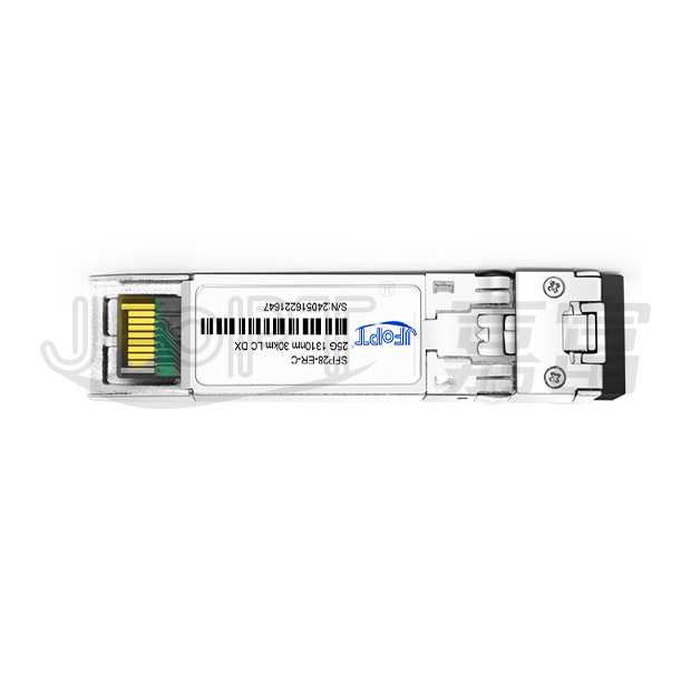
JFTSM-SFP28-25-13-30(ER)-LCD
|
Manufacturer brand
|
JFOPT
|
|
Package type
|
SFP28
|
Optical connector
|
Duplex LC
|
|
Max data rate
|
25.78G
|
Channel data rate
|
10.31Gbps
|
|
Effective transmission distance
|
30km
|
||
|
Wavelength
|
1310nm
|
Operating voltage
|
3.3V
|
|
Fiber type
|
SMF
|
Core size
|
9/125
|
|
Transmitter type
|
DML
|
Receiver type
|
APD
|
|
TX power
|
-0.5~6.5dBm
|
Receiver sensitivity
|
<19.5dBm
|
|
Digital diagnostic monitoring(DDM)
|
YES
|
Receiver overload
|
-5dBm
|
|
Power consumption
|
≤2W
|
Protocols
|
SFF-8472, SFF-8432, SFF-8431
|
|
Operating temperature(Commercial)
|
0℃~+70℃
|
Storage temperature(Commercial)
|
-40℃~+85℃
|
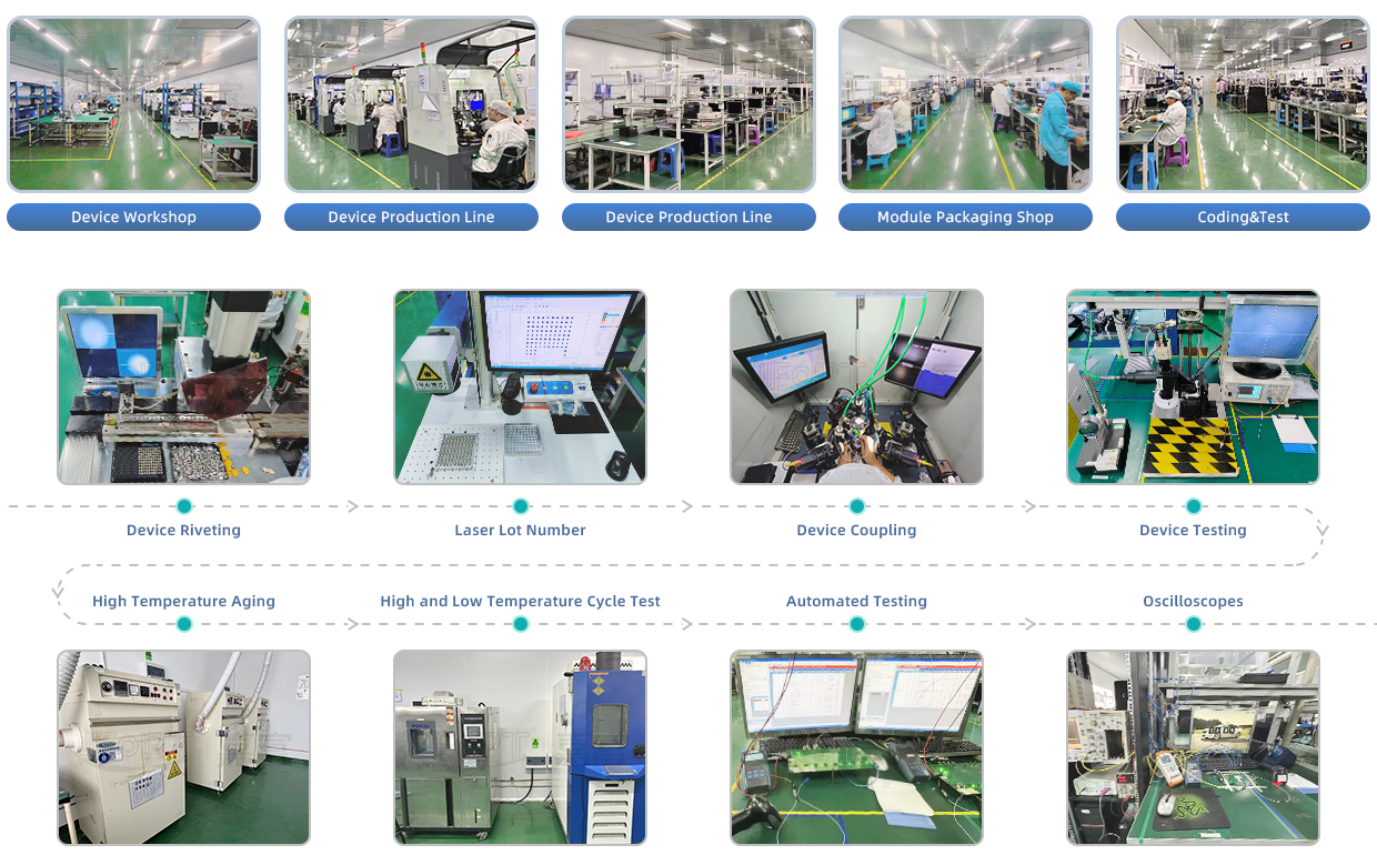
JFOPT continues to invest in optical transceiver production, covering a full range of optical transceiver such as 1*9, SFP, 10G, 25G, 100G, 200G, 400G, 800G GPON/EPON/XG/XGSPON OLT transceiver. At the same time, our company provides TOSA, ROSA, BOSA semi-finished device solutions for the downstream peer. JFOPT's production line has a daily production capacity of 10,000 optical transceivers and 20,000 optical devices. In addition, JFOPT's optical transceiver have industry-leading high temperature resistance and anti-interference capability, and are widely used in computing centers, operators, traffic security, power facilities and other industries.
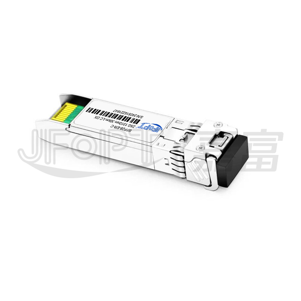
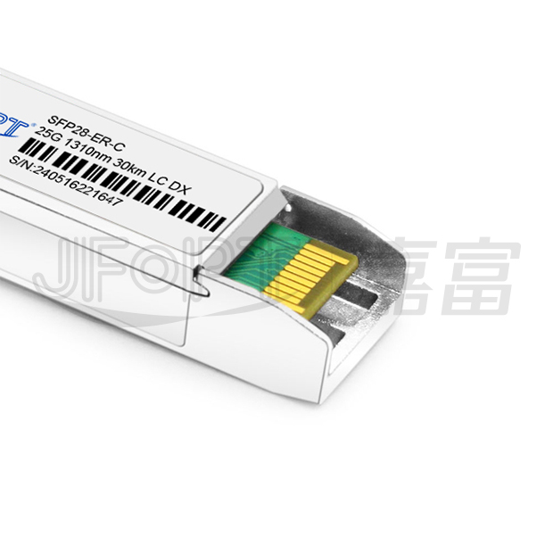
The JFOPT SFP28 25G 1310nm 30km ER LC DX transceiver is specifically designed for Ethernet links, supporting data rates of up to 25.78 Gb/s and a transmission distance of up to 30km without FEC. It adheres to SFF-8472 standards and is compatible with SFF-8432 and relevant sections of SFF-8431. Additionally, the product is RoHS-compliant and lead-free in accordance with Directive 2011/96/EU.
| UP to 25.78Gb/s data links | Hot-pluggable SFP28 footprint | ||||||||
| Duplex LC connector | DML laser transmitter, APD photo detector | ||||||||
| Up to 30km on SMF without FEC | Single 3.3V power supply | ||||||||
| Operating case temperature range: 0~ 70°C | 2-wire interface for management specifications compliant with SFF 8472 digital diagnostic monitoring interface for optical transceivers |
| High-speed storage area networks | CPRI 10 |

| Parameter | Symbol | Min. | Typ. | Max. | Unit | ||||
| Storage temperature | TS | -40 | - | 85 | °C | ||||
| Case operating temperature | TA | 0 | - | 70 | °C | ||||
| Maximum supply voltage | Vcc | 0 | - | 3.6 | V | ||||
| Relative humidity | RH | 0 | - | 85 | % | ||||
| Parameter | Symbol | Min. | Typ. | Max. | Unit | Note | |||
| Supply voltage | VCC | 3.15 | - | 3.46 | V | - | |||
| Supply current | Icc | - | - | 450 | mA | - | |||
| Power consumption | P | - | - | 1.5 | W | - | |||
| Data rate | R | - | 25.8 | - | Gb/s | - | |||
Transmitter |
|||||||||
| Input differential impedance | Rin | - | 100 | - | Ω | 1 | |||
| Differential input voltage swing | Vin,pp | 180 | - | 700 | mV | 2 | |||
| Transmit disable voltage | VD | 2 | - | Vcc | V | 3 | |||
| Transmit enable voltage | VEN | Vee | - | Vee+0.8 | V | - | |||
Receiver |
|||||||||
| Single ended output voltage tolerance |
V | -0.3 | - | 4 | V | - | |||
| Rx output diff voltage | Vo | 185 | - | 800 | mV | - | |||
| LOS fault | VLOS fault | 2 | - | VccHOST | V | 4 | |||
| LOS normal | VLOS norm | Vee | - | Vee+0.8 | V | 4 | |||
| Notes: 1.Connected directly to TX data input pins. AC coupling from pins into laser driver IC. 2.Per SFF-8431 Rev 3.0 3.Into 100 ohms differential termination. 4.LOS is an open collector output. Should be pulled up with 4.7k – 10kΩ on the host board. Normal operation is logic 0; loss of signal is logic 1. Maximum pull-up voltage is 5.5V. |
|||||||||
| Parameter | Symbol | Min. | Typ. | Max | Unit | Notes | |||
Transmitter |
|||||||||
| Center wavelength | λt | 1295 | - | 1325 | nm | - | |||
| Spectral width | △λ | - | - | 1 | nm | - | |||
| Average optical power | Pavg | 0 | - | +6 | dBm | 1 | |||
| Laser off power | Poff | - | - | -30 | dBm | - | |||
| Side mode suppression ratio | - | 30 | - | - | - | - | |||
| Extinction ratio | ER | 4 | - | - | dB | - | |||
| Optical return loss tolerance | - | - | - | -12 | dB | - | |||
Receiver |
|||||||||
| Center wavelength | λr | 1260 | - | 1370 | nm | - | |||
| Receiver sensitivity | Sen | - | - | -19 | dBm | 2 | |||
| Los assert | LOSA | -30 | - | dBm | - | ||||
| Los dessert | LOSD | - | - | -19 | dBm | - | |||
| Los hysteresis | LOSH | 0.5 | - | dB | - | ||||
| Overload | - | -6 | - | - | dBm | - | |||
Notes: 1.Average power figures are informative only, per IEEE802.3CC. 2.Receiver sensitivity is informative. Shall be measured with conformance test signal for . BER =5x 10⁻⁵. |
|||||||||
| Parameter | Symbol | Min. | Typ. | Max. | Unit | ||||
| TX_disable assert time | t_off | - | - | 100 | us | ||||
| TX_disable negate time | t_on | - | - | 2 | ms | ||||
| Time to initialize 2-wire interface | t_2w_start_up | - | - | 300 | ms | ||||
| Time to initialize | t_start_up | - | - | 300 | ms | ||||
| Time to initialize cooled module and time to power up a cooled module to power level II | t_start_up_cooled | - | - | 90 | s | ||||
| Time to power up to level II | t_power_level2 | - | - | 300 | ms | ||||
| Time to power down from level II | t_power_down | - | - | 300 | ms | ||||
| Tx_fault assert | Tx_Fault_on | - | - | 1 | ms | ||||
| Tx_fault assert for cooled module | Tx_Fault_on_cooled | - | - | 50 | ms | ||||
| TX_FAULT reset | t_reset | 10 | - | - | us | ||||
| Rx_LOS assert delay | t_los_on | - | - | 100 | us | ||||
| Rx_LOS negate delay | t_los_off | - | - | 100 | us | ||||
| Parameter | Symbol | Min. | Max. | Accuracy | Unit | ||||
| Transceiver temperature | T | 0 | +70 | ±3.0°C | °C | ||||
| Transceiver supply voltage | DDVoltage | 3.15 | 3.45 | ±3% | V | ||||
| Transmitter bias current | DDBias | 0 | 35 | ±10% | mA | ||||
| Transmitter output power | DDTx-Power | -5 | +5 | ±2dB | dBm | ||||
| Receiver average optical input power | DDRx-Power | -16 | -3 | ±2dB | dBm | ||||
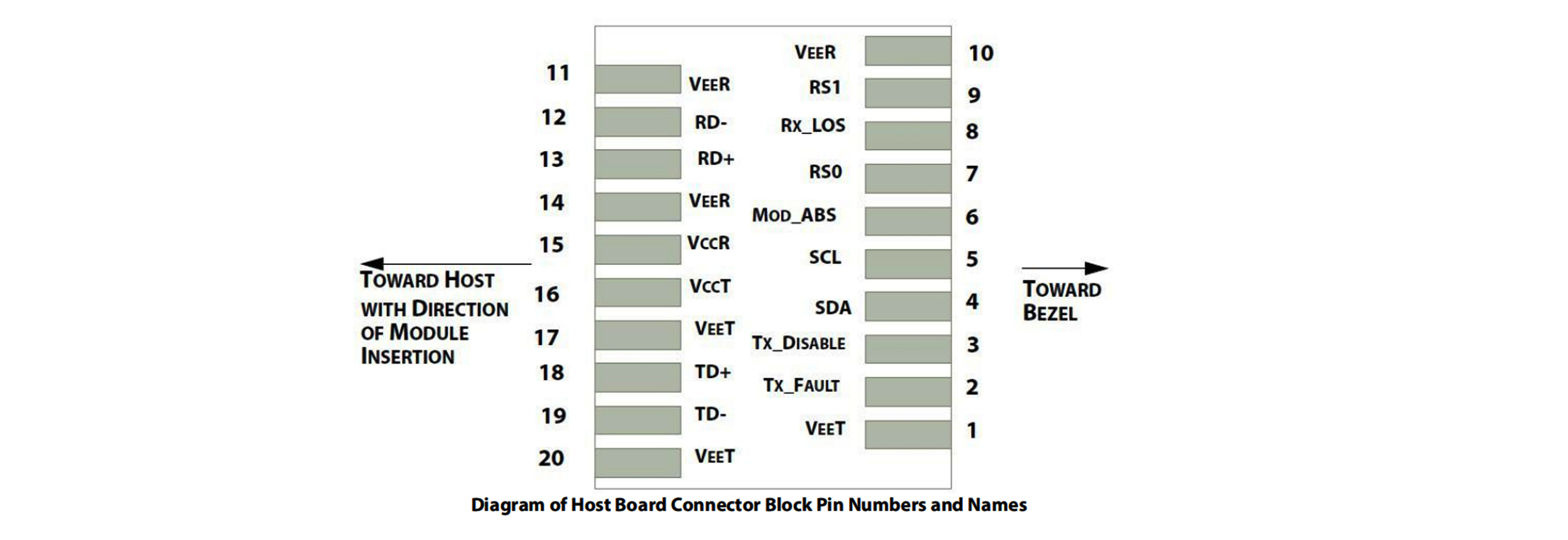
| Pin | Symbol | Name/Description | Plug Seq. | ||||||
| 1 | VeeT | Module transmitter ground | 1 | ||||||
| 2 | TX fault | Module transmitter fault | 2 | ||||||
| 3 | TX disable | Transmitter disable; turns off transmitter laser output | 3 | ||||||
| 4 | SDL | 2 wire serial interface data input/output (SDA) | 4 | ||||||
| 5 | SCL | 2 wire serial interface clock input (SCL) | 4 | ||||||
| 6 | MOD_ABS | Module absent, connect to VeeR or VeeT in the module | 2 | ||||||
| 7 | RS0 | Rate select0: module inputs and are pulled low to VeeT with >30 kΩ resistorsin the module. | - | ||||||
| 8 | LOS | Receiver Loss of signal indication | - | ||||||
| 9 | RS1 | Rate select1: module inputs and are pulled low to VeeT with >30 kΩ resistorsin the module. | - | ||||||
| 10 | VeeR | Module receiver ground | 1 | ||||||
| 11 | VeeR | Module receiver ground | 1 | ||||||
| 12 | RD- | Receiver inverted data out put | - | ||||||
| 13 | RD+ | Receiver non-inverted data out put | - | ||||||
| 14 | VeeR | Module receiver ground | 1 | ||||||
| 15 | VccR | Module receiver 3.3V supply | - | ||||||
| 16 | VccT | Module transmitter 3.3V supply | - | ||||||
| 17 | VeeT | Module transmitter ground | 1 | ||||||
| 18 | TD+ | Transmitter non-inverted data out put | - | ||||||
| 19 | TD- | Transmitter inverted data out put | - | ||||||
| 20 | VeeT | Module transmitter ground | 1 | ||||||
| Notes: 1.The module ground pins shall be isolated from the module case. 2.This pin is an open collector/drain output pin and shall be pulled up with 4.7K-10Kohms to Host_Vcc on the host board. 3.This pin shall be pulled up with 4.7K-10Kohms to VccT in the module. 4.This pin is an open collector/drain output pin and shall be pulled up with 4.7K-10Kohms to Host_Vcc on the host board. |
|||||||||


 Ann
Ann


