


| Product model | JFTSM-SFP28-25-85-01(SR)-LCD | Manufacturer brand | JFOPT |
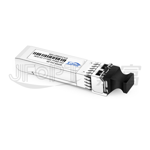
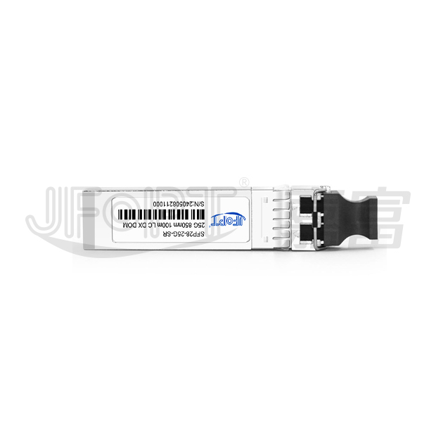
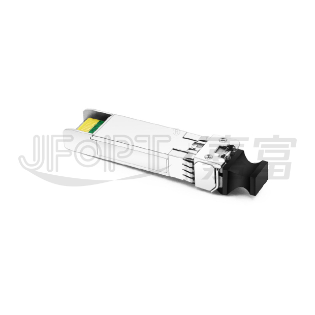
| Package type | SFP28 | Optical connector | Duplex LC |
| Max data rate | 25.78G | Channel data rate | 10.31Gbps |
| Effective transmission distance(OM3) | 70m | Effective transmission distance(OM4) | 100m |
| Wavelength | 850nm | Operating voltage | 3.3V |
| Fiber type | MMF | Core size | 50/125 |
| Transmitter type | VCSEL | Receiver type | PIN |
| TX power | -8.4~2.4dbm | Receiver sensitivity | <-6dBm |
| Digital optical monitoring(DOM) | YES | Receiver overload | 2.4dBm |
| Power consumption | ≤1W | Protocols | SFF-8472, SFF-8024, SFF-8431, SFF-8432 |
| Operating temperature(Commercial) | 0℃~+70℃ | Storage temperature(Commercial) | -40℃~+85℃ |
| Operating temperature(Industrial) | -40℃~+85℃ | Storage temperature(Industrial) | -40℃~+85℃ |
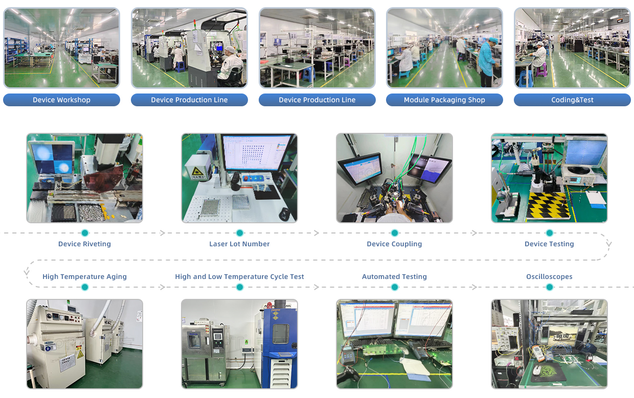
PRODUCTION LINE INTRODUCTION
JFOPT continues to invest in optical transceiver production, covering a full range of optical transceiver such as 1*9, SFP, 10G, 25G, 100G, 200G, 400G, 800G GPON/EPON/XG/XGSPON OLT transceiver. At the same time, our company provides TOSA, ROSA, BOSA semi-finished device solutions for the downstream peer. JFOPT's production line has a daily production capacity of 10,000 optical transceivers and 20,000 optical devices. In addition, JFOPT's optical transceiver have industry-leading high temperature resistance and anti-interference capability, and are widely used in computing centers, operators, traffic security, power facilities and other industries.
PRODUCT PRESENTATION
The JFOPT SFP28 25G 850nm 100m SR LC DX transceiver is optimized for 25.78Gbps data transmission over multimode fiber. Fully compliant with the SFF-8431 standard, its SFP+ mechanical design is compatible with the SFF-8432 specification.This module supports digital diagnostic monitoring through a 2-wire serial interface, as outlined in the SFF-8472 standard, ensuring precise performance monitoring and simplified network management.
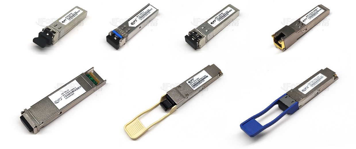
TRANSCEIVER SERIES PRODUCTS
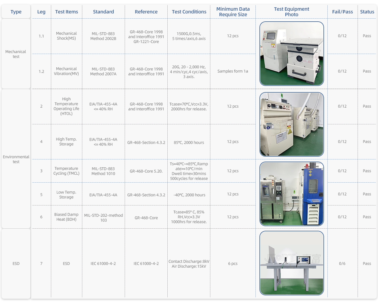
PRODUCTION & TESTING EQUIPMENT
FEATURES
| Supports 25.78Gb/s bit rate | Hot-pluggable SFP+ footprint | ||||||||
| 850nm VCSEL laser and PIN photo-detector | Internal CDR on transmitter and receiver channel | ||||||||
| Programmable RX pre-emphasis | Programmable TX input equalizer | ||||||||
| 0℃ to 70℃ operating temperature range | Link lengths at 25.78G 100m over OM4 MMF | ||||||||
| Single +3.3V±5% power supply |
APPLICATION
| 25GBASE-SR ethernet |
STANDARD COMPLIANCE

ABSOLUTE MAXIMUM RATINGS
| Parameter | Symbol | Min. | Max. | Unit | |||||
| Supply voltage | Vcc | -0.3 | +4.0 | V | |||||
| Storage temperature | Ts | -40 | +85 | ℃ | |||||
| Operating humidity | RH | 0 | +85 | % | |||||
GENERAL SPECIFICATIONS
| Parameter | Symbol | Min | Typ. | Max | Unit | ||||
| Bit rate | BR | - | 25.78 | - | Gbps | ||||
| Bit Error ratio | BER | - | - | 5*10E-5 | - | ||||
| Max. supported link length | LMax | - | - | 100 | m | ||||
RECOMMENDED OPERATING CONDITIONS
| Parameter | Symbol | Min. | Typ. | Max. | Unit | ||||
| Operating temperature | Tc | 0 | - | +70 | °C | ||||
| Power supply voltage | Vcc | 3.1 | 3.3 | 3.46 | V | ||||
| Bit rate | BR | - | 25.78 | - | Gbps | ||||
| Max. supported link length | LMAX | - | - | 100 | m | ||||
ELECTRICAL CHARACTERISTICS
| Parameter | Symbol | Min. | Typ. | Max | Unit | Note | |||
| Supply voltage | Vcc | 3.14 | 3.3 | 3.46 | V | - | |||
| Supply current | Icc | - | - | 230 | mA | - | |||
Transmitter |
|||||||||
| Input differential impedance | RIN | 80 | 100 | 120 | Ω | 1 | |||
| Single ended data input swing | VIN | 90 | - | 150 | mVp-p | - | |||
| Transmit disable voltage | VDIS | 2 | - | VCCHOST | V | - | |||
| Transmit enable voltage | VEN | VEE | - | VEE+0.8 | V | - | |||
| Transmit fault assert voltage | VFA | 2 | - | VCCHOST | V | - | |||
| Transmit fault de-assert voltage | VFDA | VEE | - | VEE+0.8 | V | - | |||
Receiver |
|||||||||
| Single ended data output swing | VOD | 200 | - | 500 | mVpp | - | |||
| LOS fault | VLOSFT | 2 | - | VCCHOST | V | - | |||
| LOS normal | VLOSFT | VEE | - | VEE+0.8 | V | - | |||
OPTICAL CHARACTERISTICS
| Parameter | Symbol | Min. | Typ. | Max. | Unit | Note | |||
Transmitter |
|||||||||
| Nominal wavelength | λ | 840 | - | 860 | nm | - | |||
| Spectral width | ∆λ | - | - | 0.6 | nm | - | |||
| Optical modulation amplitude | POMA | -6.4 | - | 3 | dBm | - | |||
| Optical output power | POFF | -8.4 | - | 2.4 | dBm | - | |||
| Extinction ratio | ER | 2 | - | - | dB | - | |||
| Transmitter dispersion penalty | TDP | - | - | 5 | dB | - | |||
| Average launch power of OFF Transmitter |
POFF | - | - | -30 | dBm | - | |||
Receiver |
|||||||||
| Center wavelength | λ | 840 | - | 860 | nm | - | |||
| Average receiver power | PAVG | -10.3 | - | 2.4 | dBm | 1 | |||
| Stressed receiver sensitivity(OMA) | RSENSE | - | - | -5.2 | dBm | 2 | |||
| Receiver reflectance | RREFL | - | - | -12 | dB | - | |||
| Assert LOS | LOSA | -30 | - | - | dBm | - | |||
| De-assert LOS | LOSD | - | - | -13 | dBm | - | |||
| LOS hysteresis | 0.5 | dB | - | ||||||
| Notes: 1. Sensitivity for 25.78G PRBS 231-1 and BER better than or equal to 5*10E-5. 2. The stressed sensitivity values in the table are for system level BER measurements which include the effects of CDR circuit. |
|||||||||
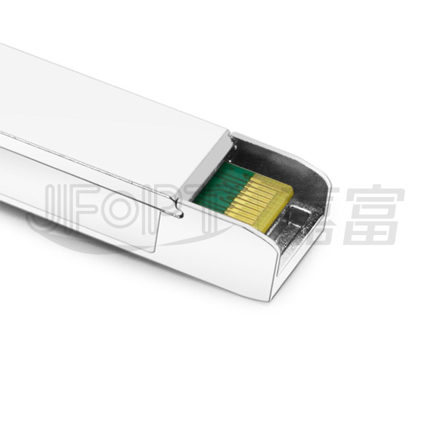
PIN ASSIGNMENT

| Pin Number | Symbol | Name | Description | ||||||
| 1,17,20 | VeeT | Transmitter signal ground | These pins should be connected to signal groundon the host board. | ||||||
| 2 | TX fault | Transmitter fault out (OC) | Logic “1” output = Transmitter fault Logic “0” output = Normal operation This pin is open collector compatible, and should be pulled up to host Vcc with a 10kΩ resistor. |
||||||
| 3 | TX disable | Transmitter disable in (LVTTL) | Logic “1” input (or no connection) = Laser off Logic “0” Input = Laser on This pin is internally pulled up to VccT with a 10 kΩ resistor |
||||||
| 4 | SDA | Module definition identifiers | Serial ID with SFF 8472 diagnostics module definition pins should be pulled up to Host Vcc with 10 kΩ resistors. | ||||||
| 5 | SCL | ||||||||
| 6 | MOD-ABS | ||||||||
| 7 | RS0 | Receiver rate select (LVTTL) Transmitter rate select (LVTTL) |
NA | ||||||
| 9 | RS1 | NA | |||||||
| 8 | LOS | Loss of signal out (OC) | This pin is open collector compatible, and should be pulled up to host Vcc with a 10kΩ resist |
||||||
| 10,11,14 | VeeR | Receiver signal ground | These pins should be connected to signal groundon the host board. | ||||||
| 12 | RD- | Receiver negative DATA out (CML) | Light on = logic “0” output receiver DATA output is internally AC coupled and series terminated with a 50Ω resistor. | ||||||
| 13 | RD+ | Receiver positive DATA out(CML) | Light on = Logic “1” output receiver DATA output is internal ly AC coupled and series terminated with a 50 Ω resistor. |
||||||
| 15 | VccR | Receiver power supply | This pin should be connected to a filtered +3.3V power supply on the host board. See figure 3.recommended power supply filter | ||||||
| 16 | VccT | Transmitter power supply | This pin should be connected to a filtered +3.3V power supply on the host board. See figure 3.recommended power supply filter | ||||||
| 18 | TD+ |
Transmitter positive DATA in(CML)
|
Logic “1” input = light on transmitter DATA inputs are internally AC coupled and terminated with a differential 100Ω resistor. | ||||||
| 19 | TD- | Transmitter negative DATA in(CML) | Logic “0” input = light on transmitter DATA inputs are internally AC coupled and terminated with a differential 100Ω resistor. | ||||||
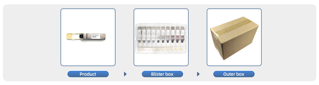
PRODUCT PACKAGING
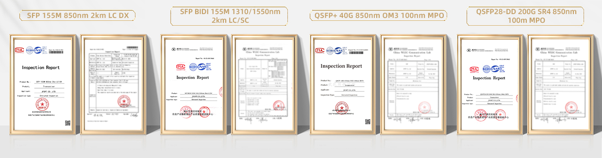
PRODUCT CERTIFICATION
QUALITY ADVANTAGE
COMPATIBLE BRANDS


 Ann
Ann


