


|
Product model
|
JFTSM-QSFP+40-85-015(SR)-MPO8/12
|
Manufacturer brand
|
JFOPT
|
|
Package type
|
QSFP+
|
Optical connector
|
MPO 8C/12C
|
|
Max data rate
|
40G
|
Channel data rate
|
10.3125Gbps
|
|
Effective transmission distance(OM3)
|
100m
|
Effective transmission distance(OM4)
|
150m
|
|
Wavelength
|
850nm
|
Operating voltage
|
3.3V
|
|
Fiber type
|
MMF
|
Core size
|
50/125
|
|
Transmitter type
|
VCSEL
|
Receiver type
|
PIN
|
|
TX power
|
-7.6~2.4dbm
|
Receiver sensitivity
|
-5.4dbm
|
|
Digital diagnostic monitoring(DDM)
|
YES
|
Receiver overload
|
2.4dBm
|
|
Power consumption
|
< 1.5W
|
Protocols
|
IEEE 802.3ba
IEEE 802.3ae
QSFP+ MSA SFF-8436
|
|
Operating temperature(Commercial)
|
0℃~+70℃
|
Storage temperature(Commercial)
|
-40℃~+85℃
|
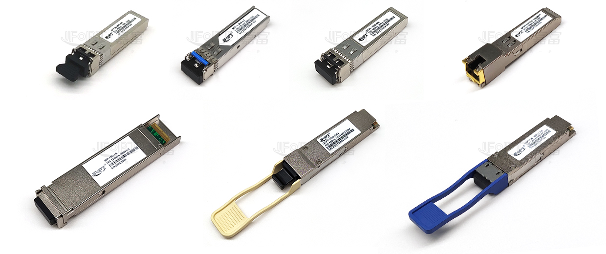
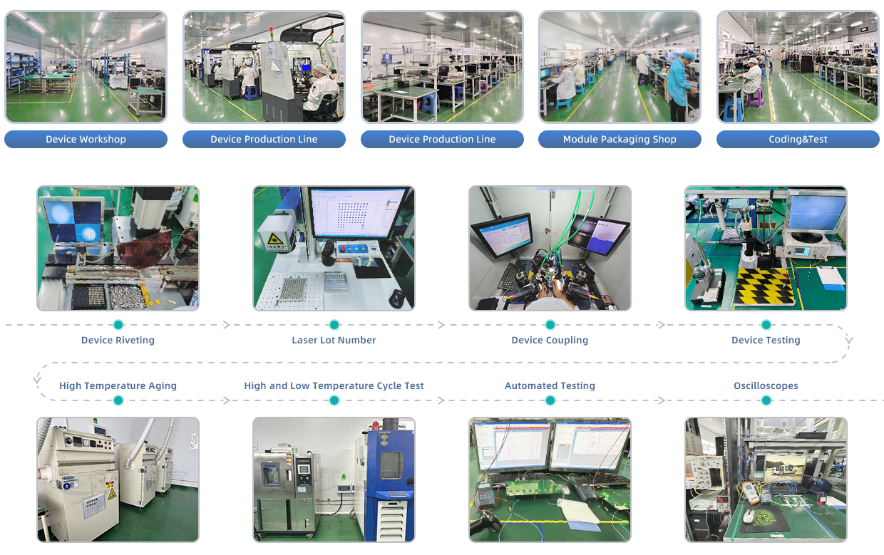
JFOPT continues to invest in optical transceiver production, covering a full range of optical transceiver such as 1*9, SFP, 10G, 25G, 100G, 200G, 400G, 800G GPON/EPON/XG/XGSPON OLT transceiver. At the same time, our company provides TOSA, ROSA, BOSA semi-finished device solutions for the downstream peer. JFOPT's production line has a daily production capacity of 10,000 optical transceivers and 20,000 optical devices. In addition, JFOPT's optical transceiver have industry-leading high temperature resistance and anti-interference capability, and are widely used in computing centers, operators, traffic security, power facilities and other industries.
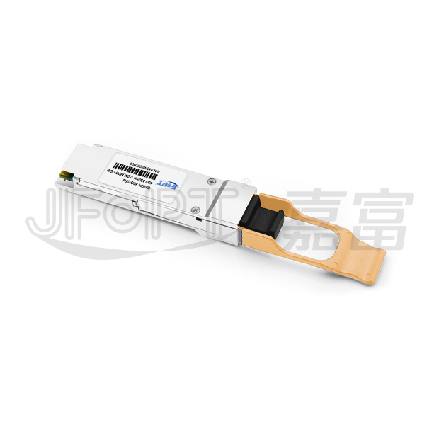
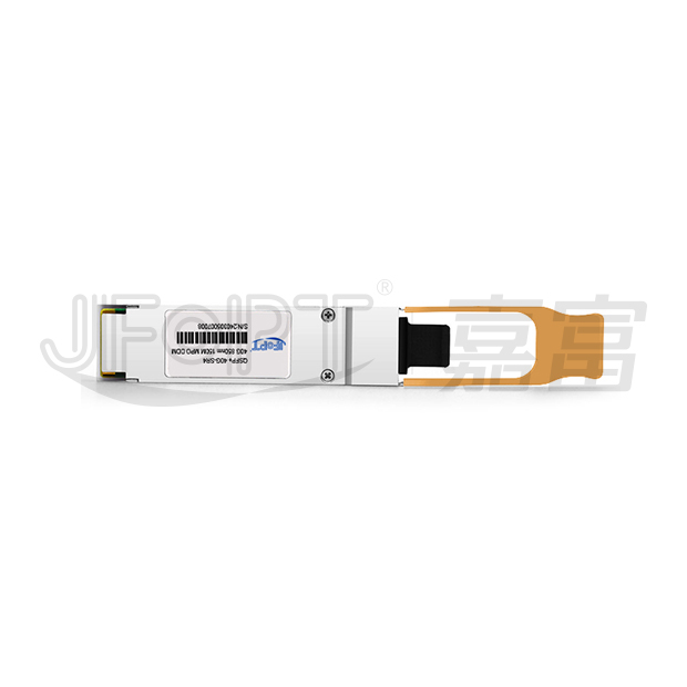
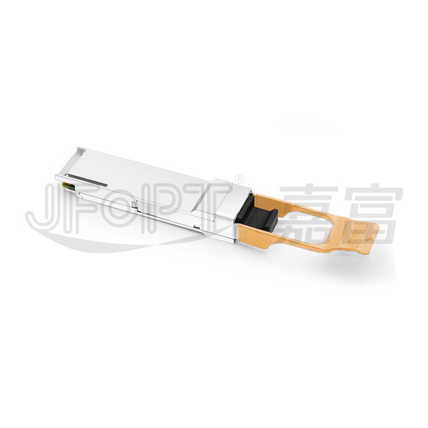
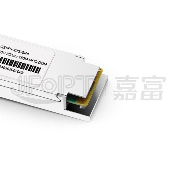
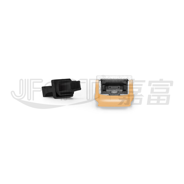
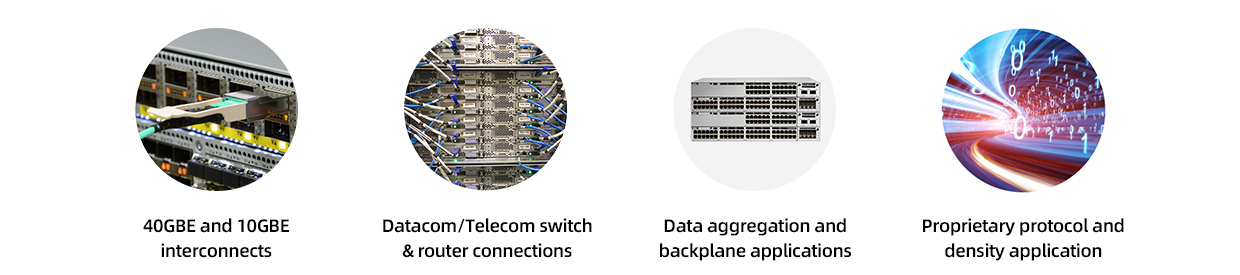
The JFOPT QSFP+ 40G 850nm 150m SR MPO 8/12 transceiver features 12-fiber MTP/MPO male connectors, supporting links up to 150m over OM4 MMF and 100m over OM3. It complies with QSFP+ MSA, IEEE 802.3ba 40GBASE-SR4, and supports 4x10GBASE-SR breakout. Fully interoperable with standard 40GBASE-SR4 interfaces, it also offers digital diagnostics via the I2C interface, per QSFP+ MSA specifications, providing real-time access to operating parameters. Its hot-swappable and easy-to-install design makes it perfect for a wide range of applications, including campus networks, data centers, cloud deployments, HPC environments, and interconnections between switches, routers, servers, and transport equipment.
| Compliant to the IEEE 802.3ba(40GBASE-SR4) | Support interoperability with IEEE 802.3ae,10GBASE-SR modules of various form factors such as SFP+, XFP, X21 | ||||||||
| Compliant to the QSFP+ MSA SFF-8436 Specification | Up to 100m on OM3 and 150m on OM4 MMF | ||||||||
| VCSEL array transmitter and PIN array receiver | Single 3.3V Power Supply and Power dissipation < 1.5W | ||||||||
| Operates at 10.3125Gbps per channel | Operating Case Temperature: 0℃~+70℃ | ||||||||
| I2C interface with integrated Digital Diagnostic Monitoring | Utilizes a standard 12/8 lane optical fiber with MPO connector | ||||||||
| Safety Certification: TUV/UL/FDA |

| Parameter | Symbol | Min. | Max. | Unit | ||||
| Storage Temperature | TS | -40 | +85 | °C | ||||
| Supply Voltage | VCC | -0.5 | 3.6 | V | ||||
| Operating Relative Humidity | RH | 5 | 85 | % | ||||
| *Exceeding any one of these values may destroy the device immediately. |
||||||||
| Parameter | Symbol | Min. | Typical | Max. | Unit | |||
| Operating Case Temperature | Tc | JFTSM-QSFP+40-85-015(SR)-MPO8/12 | 0 | +70 | °C | |||
| Power Supply Voltage | Vcc | 3.135 | 3.3 | 3.465 | V | |||
| Power Supply Current | Icc | 450 | mA | |||||
| Aggregate Bit Rate | BRAVE | 41.25 | Gbps | |||||
| Lane Bit Rate | BRLANE | 10.3125 | Gbps | |||||
| Parameter |
Symbol
|
Min. | Typical | Max. | Unit | |||
| OM3 MMF | L | 0.5 | - | 100 | m | |||
| Aggregate Bit Rate | BRAVE | - | 40 | - | Gbps | |||
| Per Lane Bit Rate | BRLANE | - | 10.3125 | - | Gbps | |||
Transmitter |
||||||||
| Center Wavelength | λC | 840 | 850 | 860 | nm | |||
| RMS Spectral Width | RMS | - | - | 0.65 | nm | |||
| Average Launch Power, Each Lane | Pout/lane | -7.6 | - | 2.4 | dBm | |||
| Transmit OMA, Per Lane | TX_OMA/lane | -5.6 | - | 3 | dBm | |||
| Difference in Launch Power Between Any Two Lanes(OMA) | - | - | 4 | dB | ||||
| Peak Power, Each Lane | - | - | 4 | dBm | ||||
| Transmitter and Dispersion Penalty,Each Lane | TDP/lane | - | - | 3.5 | dB | |||
| Extinction Ratio | ER | 3 | - | - | dB | |||
| Optical Return Loss Tolerance | - | - | 12 | dB | ||||
| Average Launch Power of OFF, Each Lane | - | - | -30 | dBm | ||||
| Output Optical Eye | IEEE 802.3ba-2010 Compliant | |||||||
Receiver |
||||||||
| Center Wavelength | λC | 840 | 850 | 860 | nm | |||
| Damage Threshold | 3.4 | - | - | dB | ||||
| Stressed Receiver Sensitivity in OMA,Each Lane | Pmins | - | - | -5.4 | dBm | |||
| Maximum Receive Power, Each Lane | Pmax | - | - | 2.4 | dBm | |||
| Average Power, Each Lane | RX/lane | -9.5 | - | +2.4 | dBm | |||
| LOS De-Assert, OMA | LOSD | - | - | -7.5 | dBm | |||
| Receiver Reflectance | Rr | - | - | -12 | dB | |||
| LOS Assert | LOSA | -30 | - | - | dBm | |||
| LOS Hysteresis | 0.5 | - | - | dB | ||||
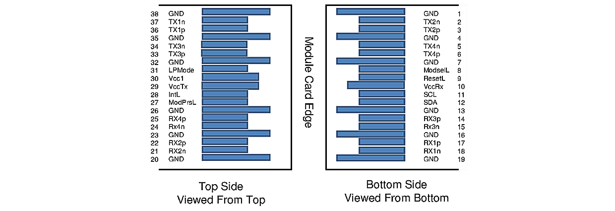
| Pin | Logic | Symbol | Description | Plug Sequence |
Notes | |||
| 1 | GND | Ground | 1 | 1 | ||||
| 2 | CML-I | Tx2n | Transmitter Inverted Data Input | 3 | ||||
| 3 | CML-I | Tx2p | Transmitter Non-Inverted Data Input | 3 | ||||
| 4 | GND | Ground | 1 | 1 | ||||
| 5 | CML-I | Tx4n | Transmitter Inverted Data Input | 3 | ||||
| 6 | CML-I | Tx4p | Transmitter Non-Inverted Data Input | 3 | ||||
| 7 | GND | Ground | 1 | 1 | ||||
| 8 | LVTTL-I | ModSelL | Module Select | 3 | ||||
| 9 | LVTTL-I | ResetL | Module Reset | 3 | ||||
| 10 | VccRx | +3.3V Power Supply Receiver | 2 | 2 | ||||
| 11 | LVCMOS- I/O | SCL | 2-wire Serial Interface Clock | 3 | ||||
| 12 | LVCMOS- I/O | SDA | 2-wire Serial Interface Data | 3 | ||||
| 13 | GND | Ground | 1 | 1 | ||||
| 14 | CML-O | Rx3p | Receiver Non-Inverted Data Output | 3 | ||||
| 15 | CML-O | Rx3n | Receiver Inverted Data Output | 3 | ||||
| 16 | GND | Ground | 1 | 1 | ||||
| 17 | CML-O | Rx1p | Receiver Non-Inverted Data Output | 3 | ||||
| 18 | CML-O | Rx1n | Receiver Inverted Data Output | 3 | ||||
| 19 | GND | Ground | 1 | 1 | ||||
| 20 | GND | Ground | 1 | 1 | ||||
| 21 | CML-O | Rx2n | Receiver Inverted Data Output | 3 | ||||
| 22 | CML-O | Rx2p | Receiver Non-Inverted Data Output | 3 | ||||
| 23 | GND | Ground | 1 | 1 | ||||
| 24 | CML-O | Rx4n | Receiver Inverted Data Output | 3 | ||||
| 25 | CML-O | Rx4p | Receiver Non-Inverted Data Output | 3 | ||||
| 26 | GND | Ground | 1 | 1 | ||||
| 27 | LVTTL-O | ModPrsL | Module Present | 3 | ||||
| 28 | LVTTL-O | IntL | Interrupt | 3 | ||||
| 29 | VccTx | +3.3V Power supply transmitter | 2 | 2 | ||||
| 30 | Vcc1 | +3.3V Power supply | 2 | 2 | ||||
| 31 | LVTTL-I | LPMode | Low Power Mode | 3 | ||||
| 32 | GND | Ground | 1 | 1 | ||||
| 33 | CML-I | Tx3p | Transmitter Non-Inverted Data Input | 3 | ||||
| 34 | CML-I | Tx3n | Transmitter Inverted Data Input | 3 | ||||
| 35 | GND | Ground | 1 | 1 | ||||
| 36 | CML-I | Tx1p | Transmitter Non-Inverted Data Input | 3 | ||||
| 37 | CML-I | Tx1n | Transmitter Inverted Data Input | 3 | ||||
| 38 | GND | Ground | 1 | 1 | ||||
1: GND is the symbol for signal and supply (power) common for the QSFP+ module. All are common within the QSFP+ module and all module voltages are referenced to this potential unless otherwise noted. Connect these directly to the host board signal-common ground plane.
2: Vcc Rx, Vcc1 and Vcc Tx are the receiver and transmitter power supplies and shall be applied concurrently. Vcc Rx Vcc1 and Vcc Tx may be internally connected within the QSFP+ Module in any combination. The connector pins are each rated for a maximum current of 500mA.


 Ann
Ann


