


|
Product model
|
JFTSM-QSFP+40-CW4-10(LR4)-LCD
|
Manufacturer brand
|
JFOPT
|
|
Package type
|
QSFP+
|
Optical connector
|
LC Duplex
|
|
Max data rate
|
40Gbps
|
Channel data rate
|
10.3125Gbps
|
|
Effective transmission distance
|
20km
|
||
|
Wavelength
|
1271nm, 1291nm
1311nm, 1331nm
|
Operating voltage
|
3.3V
|
|
Fiber type
|
SMF
|
Core size
|
9/125
|
|
Transmitter type
|
DFB CWDM
|
Receiver type
|
PIN
|
|
TX power
|
-4.5~2.3dBm
|
Receiver sensitivity
|
<-12.5dBm
|
|
Digital diagnostic monitoring(DDM)
|
YES
|
Receiver overload
|
3.3dBm
|
|
Power consumption
|
Commercial≤3.5W
Industrial≤4.5W
|
Protocols
|
SFF-8436 QSFP MSA
|
|
Operating temperature(Commercial)
|
0℃~+70℃
|
Storage temperature(Commercial)
|
-40℃~+85℃
|
|
Operating temperature(Industrial)
|
-40℃~+85℃
|
Storage temperature(Industrial)
|
-40℃~+85℃
|
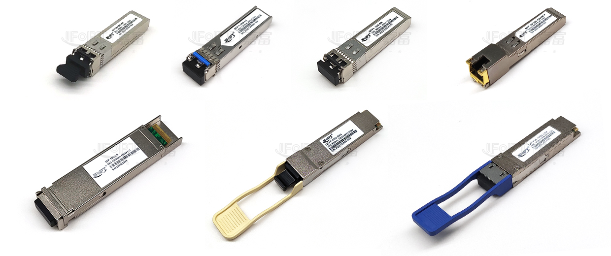
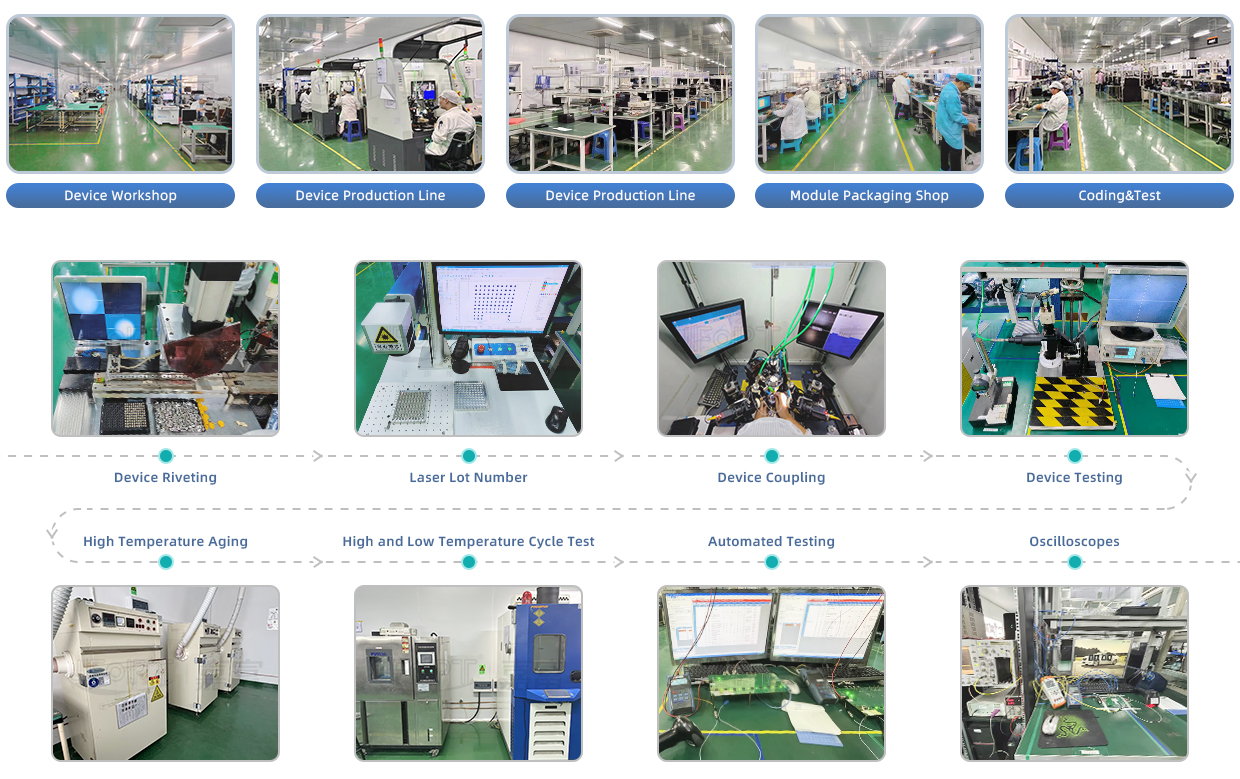
JFOPT continues to invest in optical transceiver production, covering a full range of optical transceiver such as 1*9, SFP, 10G, 25G, 100G, 200G, 400G, 800G GPON/EPON/XG/XGSPON OLT transceiver. At the same time, our company provides TOSA, ROSA, BOSA semi-finished device solutions for the downstream peer. JFOPT's production line has a daily production capacity of 10,000 optical transceivers and 20,000 optical devices. In addition, JFOPT's optical transceiver have industry-leading high temperature resistance and anti-interference capability, and are widely used in computing centers, operators, traffic security, power facilities and other industries.
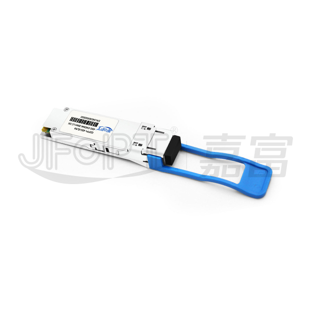
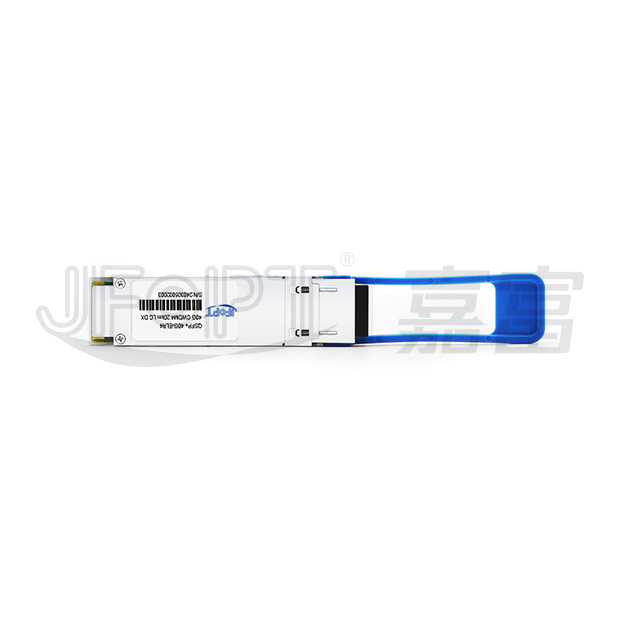
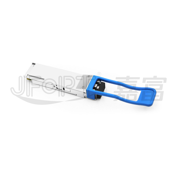
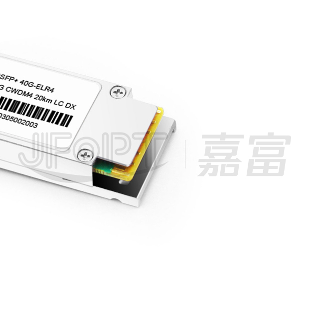
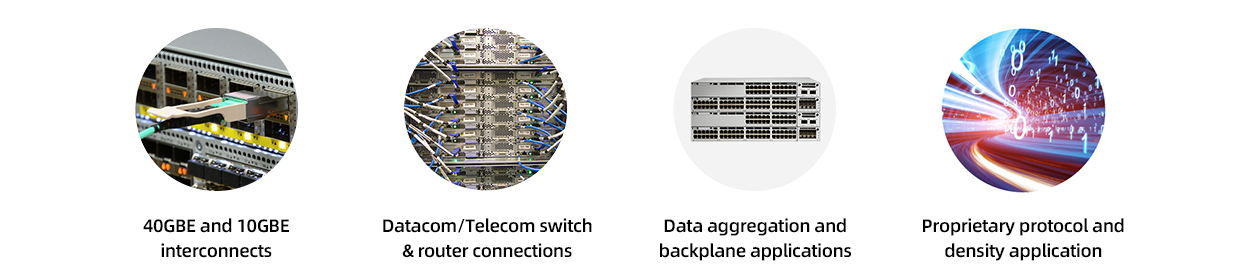
The JFOPT QSFP+ 40G CWDM4 10km LR4 LC DX transceiver is engineered for 40GBASE Ethernet connections, supporting up to 10 kilometers over single-mode fiber (SMF) at a 1310nm wavelength, using duplex LC connectors. It complies with QSFP+ MSA, IEEE 802.3ba 40GBASE-LR4, and OTU3 C4S1-2D1 standards. Additionally, it offers digital diagnostics through the I2C interface as outlined by the QSFP+ MSA, enabling real-time monitoring of operating parameters. This hot-swappable, easy-to-install transceiver is ideal for use in data centers, high-performance computing, and enterprise core and distribution networks.
| Compliant to the IEEE 802.3ba(40GBASE-LR4) | Compliant to the QSFP+ MSA SFF-8436 specification | ||||||||
| Up to 20km over SMF | DFBs and PIN monitor photodiodes array for transmitter section | ||||||||
| PIN detectors and TIAs array for receiver section | Four 10Gbps CWDM channels in the 1300nm band | ||||||||
| I2C interface with integrated digital diagnostic monitoring | Utilizes two standard LC optical connector | ||||||||
| Operating case temperature: 0℃~+70℃ |

| Parameter | Symbol | Min. | Max. | Unit | ||||
| Storage temperature | TS | -40 | +85 | °C | ||||
| Supply voltage | VCC | -0.5 | 3.6 | V | ||||
| Operating relative humidity | RH | 0 | 85 | % | ||||
*Exceeding any one of these values may destroy the device immediately.
| Parameter | Symbol | Min. | Typical | Max. | Unit | |||
| Operating case temperature | Tc | 0 | - | +70 | °C | |||
| Power supply voltage | Vcc | 3.15 | 3.3 | 3.45 | V | |||
| Power supply current | Icc | - | - | 1100 | mA | |||
| Power dissipation | PD | - | - | 3.5 | W | |||
| Aggregate bit rate | BRAVE | - | 41.25(40GE) | - | Gbps | |||
| Lane bit rate | BRLANE | - | 10.3125(40GE) | - | Gbps | |||
| Parameter | Symbol | Min. | Typ. | Max | Unit | Notes | ||
Transmitter |
||||||||
| Single ended input voltage tolerance | - | -0.3 | - | 4 | V | Referred to TP1 signal common |
||
| Differential input amplitude | - | 150 | - | 1000 | mvp-p | - | ||
| AC common mode input voltage tolerance | - | 15 | - | - | mV | RMS | ||
| Input impedance(differential) | Zin | 85 | 100 | 115 | ohms | Rin > 100 kohms @ DC |
||
| TX Disable | Disable | VIH | 2 | - | Vcc+0.3 | V | - | |
| Enable | VIL | 0 | - | 0.8 | - | |||
| TX FAULT | Fault | VOH | 2.4 | - | Vcc+0.3 | V | - | |
| Normal | VOL | 0 | - | 0.8 | - | |||
| Receiver | ||||||||
| Single ended output voltage | - | -0.3 | - | 4 |
s
|
Referred to ignal common |
||
| Differential output amplitude | - | 290 | - | 1000 | mvp-p | - | ||
| AC common mode voltage | - | - | - | 7.5 | mV | RMS | ||
| Termination mismatch at 1MHz | - | - | - | 5 | % | - | ||
| Output impedance(differential) | Zout | 85 | 100 | 115 | ohms | - | ||
| Output rise/fall time | tr/tf | 30 | - | - | ps | 10%~90% | ||
| RX_LOS | LOS | VOH | 2.4 | - | Vcc+0.3 | V | - | |
| Normal | VOL | 0 | - | 0.8 | V | - | ||
| Parameter |
Symbol
|
Min. | Typical | Max. | Unit | |||
| SMF | L | - | 10 | - | km | |||
| Aggregate bit rate | BRAVE | - | 41.25 | - | Gbps | |||
| Per lane bit rate | BRLANE | - | 10.3125 | - | Gbps | |||
Transmitter |
||||||||
| Channels wavelength | λC | 1264.5 | 1271 | 1277.5 | nm | |||
|
1284.5
|
1291 | 1297.5 | ||||||
| 1304.5 | 1311 | 1317.5 | ||||||
| 1324.5 | 1331 | 1337.5 | ||||||
| -20dB spectral width | ∆λ | - | - | 1 | nm | |||
| Average launch power, each lane | Pout/lane | -3.5 | - | 2.3 | dBm | |||
| Extinction ratio | Er | 3.5 | - | - | dB | |||
| Output optical eye | IEEE 802.3ba-2010 Compliant | |||||||
| Receiver |
||||||||
| Channels wavelength | λC | 1264.5 | 1271 | 1277.5 | nm | |||
| 1284.5 | 1291 | 1297.5 | ||||||
| 1304.5 | 1311 | 1317.5 | ||||||
| 1324.5 | 1331 | 1337.5 | ||||||
| Damage threshold | - | 5.5 | - | - | dBm | |||
| Receiver sensitivity in OMA, each lane | Pmins | - | - | -12.5 | dBm | |||
| Maximum receive power, each lane | Pmax | 2.3 | - | - | dBm | |||
| Receiver reflectance | Rr | - | - | -26 | dB | |||
| Los de-assert | LOSD | - | - | -15 | dBm | |||
| Los assert | LOSA | -24 | - | - | dBm | |||
| Los hysteresis | - | 0.5 | - | - | dB | |||

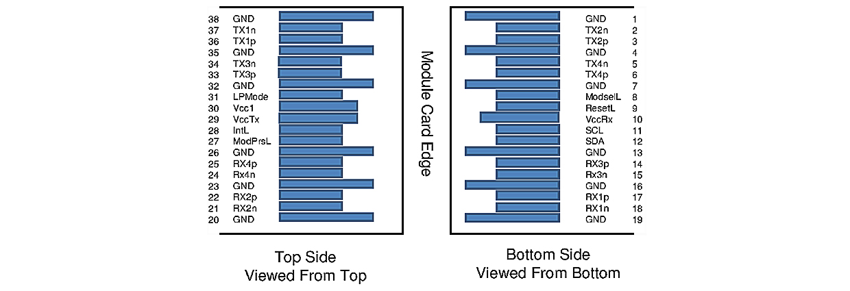
| Pin | Logic | Symbol | Description | Plug Sequence | Notes | |||
| 1 | - | GND | Ground | 1 | 1 | |||
| 2 | CML-I | Tx2n | Transmitter Inverted Data Input | 3 | - | |||
| 3 | CML-I | Tx2p | Transmitter Non-Inverted Data Input | 3 | - | |||
| 4 | - | GND | Ground | 1 | 1 | |||
| 5 | CML-I | Tx4n | Transmitter Inverted Data Input | 3 | - | |||
| 6 | CML-I | Tx4p | Transmitter Non-Inverted Data Input | 3 | - | |||
| 7 | - | GND | Ground | 1 | 1 | |||
| 8 | LVTTL-I | ModSelL | Module Select | 3 | - | |||
| 9 | LVTTL-I | ResetL |
Module Reset
|
3 | - | |||
| 10 | - | VccRx | +3.3V Power Supply Receiver | 2 | 2 | |||
| 11 | LVCMOS- I/O | SCL | 2-wire Serial Interface Clock | 3 | - | |||
| 12 | LVCMOS- I/O | SDA | 2-wire Serial Interface Data | 3 | - | |||
| 13 | - | GND | Ground | 1 | 1 | |||
| 14 | CML-O | Rx3p | Receiver Non-Inverted Data Output | 3 | - | |||
| 15 | CML-O | Rx3n | Receiver Inverted Data Output | 3 | - | |||
| 16 | - | GND | Ground | 1 | 1 | |||
| 17 | CML-O | Rx1p | Receiver Non-Inverted Data Output | 3 | - | |||
| 18 | CML-O | Rx1n | Receiver Inverted Data Output | 3 | - | |||
| 19 | - | GND | Ground | 1 | 1 | |||
| 20 | - | GND | Ground | 1 | 1 | |||
| 21 | CML-O | Rx2n | Receiver Inverted Data Output | 3 | - | |||
| 22 | CML-O | Rx2p | Receiver Non-Inverted Data Output | 3 | - | |||
| 23 | - | GND | Ground | 1 | 1 | |||
| 24 | CML-O | Rx4n | Receiver Inverted Data Output | 3 | - | |||
| 25 | CML-O | Rx4p | Receiver Non-Inverted Data Output | 3 | - | |||
| 26 | - | GND | Ground | 1 | 1 | |||
| 27 | LVTTL-O | ModPrsL | Module Present | 3 | - | |||
| 28 | LVTTL-O | IntL | Interrupt | 3 | - | |||
| 29 | - | VccTx | +3.3V Power supply transmitter | 2 | 2 | |||
| 30 | - | Vcc1 | +3.3V Power supply | 2 | 2 | |||
| 31 | LVTTL-I | LPMode | Low Power Mode | 3 | - | |||
| 32 | - | GND | Ground | 1 | 1 | |||
| 33 | CML-I | Tx3p | Transmitter Non-Inverted Data Input | 3 | - | |||
| 34 | CML-I | Tx3n | Transmitter Inverted Data Input | 3 | - | |||
| 35 | - | GND | Ground | 1 | 1 | |||
| 36 | CML-I | Tx1p | Transmitter Non-Inverted Data Input | 3 | - | |||
| 37 | CML-I | Tx1n | Transmitter Inverted Data Input | 3 | - | |||
| 38 | - | GND | Ground | 1 | 1 | |||
1: GND is the symbol for signal and supply (power) common for the QSFP+ module. All are common within the QSFP+ module and all module voltages are referenced to this potential unless otherwise noted. Connect these directly to the host board signal-common ground plane.
2: Vcc Rx, Vcc1 and Vcc Tx are the receiver and transmitter power supplies and shall be applied concurrently. Requirements defined for the host side of the Host Edge Card Connector are listed in Table 6. Recommended host board power supply filtering is shown in Figures 3 and 4. Vcc Rx Vcc1 and Vcc Tx may be internally connected within the QSFP+ Module in any combination. The connector pins are each rated for a maximum current of 500mA.


 Ann
Ann


