


|
Product model
|
JFTSM-QSFP+40-CW4-40(ER4)-LCD
|
Manufacturer brand
|
JFOPT
|
|
Package type
|
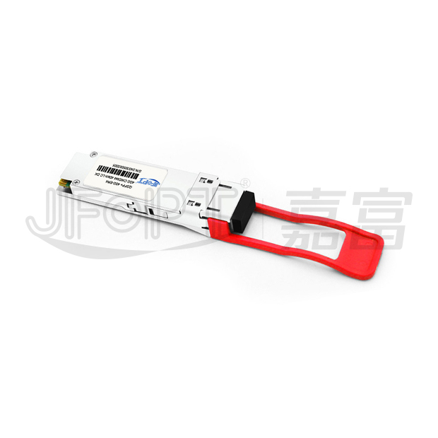
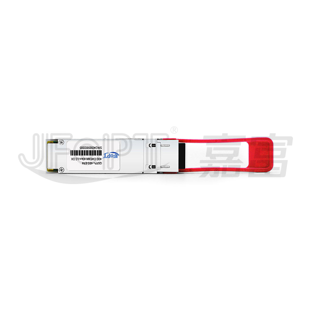
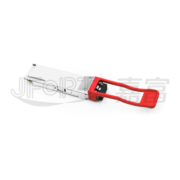
QSFP+
|
Optical connector
|
LC Duplex
|
|
Max data rate
|
40Gbps
|
Channel data rate
|
10.3125Gbps
|
|
Effective transmission distance
|
40km
|
||
|
Wavelength
|
1271nm, 1291nm
1311nm, 1331nm
|
Operating voltage
|
3.3V
|
|
Fiber type
|
SMF
|
Core size
|
9/125
|
|
Transmitter type
|
DFB CWDM
|
Receiver type
|
APD
|
|
TX power
|
-2.7~4.5dBm
|
Receiver sensitivity
|
<-21.2dBm
|
|
Digital diagnostic monitoring(DDM)
|
YES
|
Receiver overload
|
-4.5dBm
|
|
Power consumption
|
Commercial≤3.5W
Industrial≤4.5W
|
Protocols
|
IEEE 802.3ba 40GBASE-ER4
|
|
Operating temperature(Commercial)
|
0℃~+70℃
|
Storage temperature(Commercial)
|
-40℃~+85℃
|
|
Operating temperature(Industrial)
|
-40℃~+85℃
|
Storage temperature(Industrial)
|
-40℃~+85℃
|
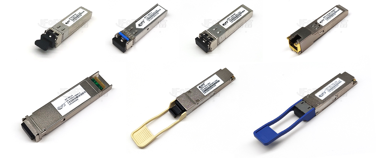
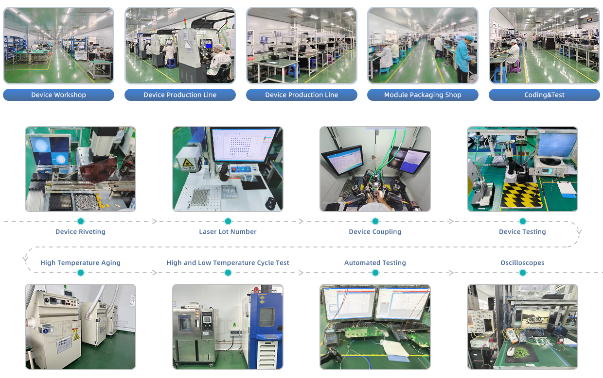
JFOPT continues to invest in optical transceiver production, covering a full range of optical transceiver such as 1*9, SFP, 10G, 25G, 100G, 200G, 400G, 800G GPON/EPON/XG/XGSPON OLT transceiver. At the same time, our company provides TOSA, ROSA, BOSA semi-finished device solutions for the downstream peer. JFOPT's production line has a daily production capacity of 10,000 optical transceivers and 20,000 optical devices. In addition, JFOPT's optical transceiver have industry-leading high temperature resistance and anti-interference capability, and are widely used in computing centers, operators, traffic security, power facilities and other industries.
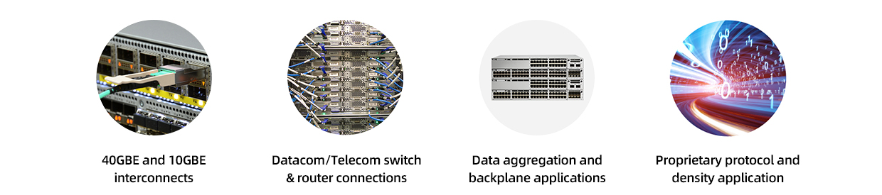
The JFOPT QSFP+ 40G CWDM4 40km ER4 LC DX transceiver module is designed for 40GbE connections over single mode fiber (SMF) with a range of up to 40km. It adheres to IEEE 802.3ba 40GBASE-ER4 standards and provides digital diagnostics via an I2C interface as outlined by the QSFP+ MSA.
| Supports 40Gbps | Single 3.3V power supply | ||||||||
| Commercial power dissipation <3.5W and and industrial power dissipation <4.5W | Up to 40km over SMF | ||||||||
|
Operating case temperature range of
Standard: 0°C to 70°C
Industrial: -40°C to 85°C
|
Four 10G DFB base CWDM channels on transmitter side | ||||||||
| Duplex LC receptacles | I2C interface with integrated digital diagnostic monitoring | ||||||||
| Safety certification: TUV/UL/FDA | RoHS compliant |

| Parameter | Symbol | Min. | Max. | Unit | ||||
| Storage temperature | TS | -40 | +85 | °C | ||||
| Supply voltage | VCC | -0.5 | 3.6 | V | ||||
| Operating relative humidity | RH | 0 | 85 | % | ||||
*Exceeding any one of these values may destroy the device immediately.
| Parameter | Symbol | Min. | Typical | Max. | Unit | |||
| Operating case temperature | Tc | QSFP+40-CW4-40(ER4)-LCD | 0 | - | +70 | °C | ||
| -40 | - | +85 | °C | |||||
| Power supply voltage | Vcc | 3.135 | 3.3 | 3.465 | V | |||
| Commercial power dissipation | PD | - | - | 3.5 | W | |||
| Industrial power dissipation | PD | - | - | 4.5 | W | |||
| Link distance with G.652 | D | - | - | 40 | km | |||
| Parameter | Symbol | Min. | Typ. | Max | Unit | Notes | ||
| Supply voltage | - | 3.1 | - | 3.47 | V | - | ||
| Supply current | Icc | - | - | 1.44 | A | - | ||
| Transmit turn-on time | - | - | - | 2000 | ms | Note3 | ||
Transmitter |
||||||||
| Differential input voltage swing |
Vin,pp | 190 | - | 700 | mVp-p | - | ||
| Input impedance (Differential) | Zin | 90 | 100 | 110 | ohms | Rin > 100 kohms @ DC |
||
Receiver |
||||||||
| Differential output voltage swing |
Vout,pp | 300 | - | 850 | mVp-p | - | ||
| AC common mode output voltage |
- | - | - | 7.5 | mV | RMS | ||
| Output impedance (Differential) |
Zout | 90 | 100 | 110 | ohms | - | ||
| Output transition time | - | 28 | - | - | ps | 20%~80% | ||
| Parameter |
Symbol
|
Min. | Typical | Max. | Unit | |||
Transmitter |
||||||||
| Signaling speed per lane | BRAVE | - | 10.3125 | 11.2 | Gbps | |||
| Side mode launch power | SMSR | 30 | - | - | dB | |||
| Total average launch power | PT | - | - | 10.5 | dBm | |||
| Lane_0 center wavelength | λC0 | 1264.5 | 1271 | 1277.5 | nm | |||
| Lane_1 center wavelength | λC1 |
1284.5
|
1291 | 1297.5 | nm | |||
| Lane_2 center wavelength | λC2 | 1304.5 | 1311 | 1317.5 | nm | |||
| Lane_3 center wavelength | λC3 | 1324.5 | 1331 | 1337.5 | nm | |||
| Average launch power per lane | Peach | -2.7 | - | 4.5 | dBm | |||
| Average launch power of OFF transmitter per lane | - | - | - | -30 | dBm | |||
| Relative intensity noise | Rin | - | - | -128 | dB/Hz | |||
| Optical modulation amplitude | Poma | 0.3 | 0 | 5.0 | dBm | |||
| Optical return loss tolerance | - | - | - | 20 | dB | |||
| Differnce in launch power between any two lanes | Ptx,diff | - | - | 4.7 | dB | |||
| Transmitter reflectance | RT | - | - | -12 | dB | |||
| Extinction ratio | ER | 5.5 | - | - | dB | |||
| Transmitter eye mask definition{X1, X2, X3, Y1, Y2, Y3} | - | {0.25 ,0.4 ,0.45 ,0.25 ,0.28 ,0.4} | - | |||||
Receiver |
||||||||
| Signaling speed per lane | BRAVE | - | 10.3125 | - | Gbps | |||
| Data rate variation | -100 | - | +100 | ppm | ||||
| Damage threshold | Rdam | 3.8 | - | - | dBm | |||
| Lane_0 center wavelength | λC0 | 1264.5 | 1271 | 1277.5 | nm | |||
| Lane_1 center wavelength | λC1 | 1284.5 | 1291 | 1297.5 | nm | |||
| Lane_2 center wavelength | λC2 | 1304.5 | 1311 | 1317.5 | nm | |||
| Lane_3 center wavelength | λC3 | 1324.5 | 1331 | 1337.5 | nm | |||
| Average receive power per lane | Rpow | -21.2 | - | -4.5 | dBm | |||
| Receiver sensitivity in OMA per lane | Pmin | - | - | -19 | dBm | |||
| Stressed receiver sensitivity (OMA) per lane | RXSRS | - | - | -16.8 | dBm | |||
Conditions of stressed receiver sensitivity test: |
||||||||
| Vertical eye closure penalty | VECP | - | 2.2 | - | dB | |||
| Stressed J2 jitter | J2 | - | 0.3 | - | UI | |||
| Stressed J9 jitter | J9 | - | 0.47 | - | UI | |||
| LOS assert | LOSA | -35 | - | - | dBm | |||
| LOS de-assert | LOSD | - | - | -23 | dBm | |||
| LOS hysteresis | - | 0.5 | - | - | dB | |||
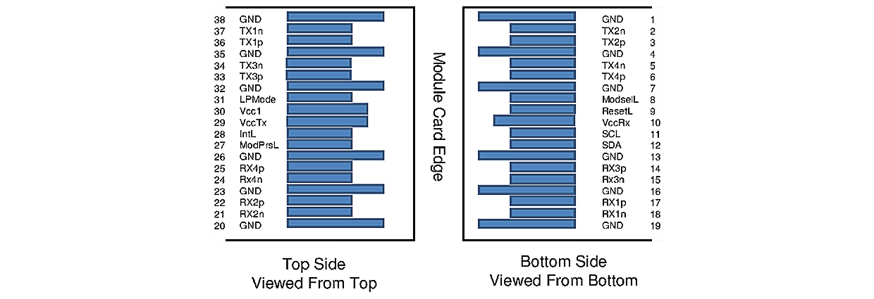
| Pin | Logic | Symbol | Description | Plug Sequence | Notes | |||
| 1 | - | GND | Ground | 1 | 1 | |||
| 2 | CML-I | Tx2n | Transmitter Inverted Data Input | 3 | - | |||
| 3 | CML-I | Tx2p | Transmitter Non-Inverted Data Input | 3 | - | |||
| 4 | - | GND | Ground | 1 | 1 | |||
| 5 | CML-I | Tx4n | Transmitter Inverted Data Input | 3 | - | |||
| 6 | CML-I | Tx4p | Transmitter Non-Inverted Data Input | 3 | - | |||
| 7 | - | GND | Ground | 1 | 1 | |||
| 8 | LVTTL-I | ModSelL | Module Select | 3 | - | |||
| 9 | LVTTL-I | ResetL |
Module Reset
|
3 | - | |||
| 10 | - | VccRx | +3.3V Power Supply Receiver | 2 | 2 | |||
| 11 | LVCMOS- I/O | SCL | 2-wire Serial Interface Clock | 3 | - | |||
| 12 | LVCMOS- I/O | SDA | 2-wire Serial Interface Data | 3 | - | |||
| 13 | - | GND | Ground | 1 | 1 | |||
| 14 | CML-O | Rx3p | Receiver Non-Inverted Data Output | 3 | - | |||
| 15 | CML-O | Rx3n | Receiver Inverted Data Output | 3 | - | |||
| 16 | - | GND | Ground | 1 | 1 | |||
| 17 | CML-O | Rx1p | Receiver Non-Inverted Data Output | 3 | - | |||
| 18 | CML-O | Rx1n | Receiver Inverted Data Output | 3 | - | |||
| 19 | - | GND | Ground | 1 | 1 | |||
| 20 | - | GND | Ground | 1 | 1 | |||
| 21 | CML-O | Rx2n | Receiver Inverted Data Output | 3 | - | |||
| 22 | CML-O | Rx2p | Receiver Non-Inverted Data Output | 3 | - | |||
| 23 | - | GND | Ground | 1 | 1 | |||
| 24 | CML-O | Rx4n | Receiver Inverted Data Output | 3 | - | |||
| 25 | CML-O | Rx4p | Receiver Non-Inverted Data Output | 3 | - | |||
| 26 | - | GND | Ground | 1 | 1 | |||
| 27 | LVTTL-O | ModPrsL | Module Present | 3 | - | |||
| 28 | LVTTL-O | IntL | Interrupt | 3 | - | |||
| 29 | - | VccTx | +3.3V Power supply transmitter | 2 | 2 | |||
| 30 | - | Vcc1 | +3.3V Power supply | 2 | 2 | |||
| 31 | LVTTL-I | LPMode | Low Power Mode | 3 | - | |||
| 32 | - | GND | Ground | 1 | 1 | |||
| 33 | CML-I | Tx3p | Transmitter Non-Inverted Data Input | 3 | - | |||
| 34 | CML-I | Tx3n | Transmitter Inverted Data Input | 3 | - | |||
| 35 | - | GND | Ground | 1 | 1 | |||
| 36 | CML-I | Tx1p | Transmitter Non-Inverted Data Input | 3 | - | |||
| 37 | CML-I | Tx1n | Transmitter Inverted Data Input | 3 | - | |||
| 38 | - | GND | Ground | 1 | 1 | |||
1: GND is the symbol for signal and supply (power) common for the QSFP+ module. All are common within the QSFP+ module and all module voltages are referenced to this potential unless otherwise noted. Connect these directly to the host board signal-common ground plane.
2: Vcc Rx, Vcc1 and Vcc Tx are the receiver and transmitter power supplies and shall be applied concurrently. Requirements defined for the host side of the Host Edge Card Connector are listed in Table 6. Recommended host board power supply filtering is shown in Figures 3 and 4. Vcc Rx Vcc1 and Vcc Tx may be internally connected within the QSFP+ Module in any combination. The connector pins are each rated for a maximum current of 500mA.


 Ann
Ann


