


|
Product model
|
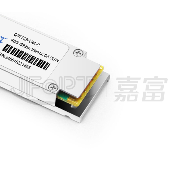
JFTSM-QSFP28-100-LW-10(LR4)-LCD-OUT4
|
Manufacturer brand
|
JFOPT
|
|
Package type
|
QSFP28
|
Optical connector
|
LC DX
|
|
Max data rate
|
112Gbps
|
Channel data rate
|
25.9525Gbps
|
|
Effective transmission distance
|
10km
|
||
|
Wavelength
|
1310nm
|
Operating voltage
|
3.3V
|
|
Fiber type
|
SMF
|
Core size
|
9/125
|
|
Transmitter type
|
DFB
|
Receiver type
|
PIN
|
|
TX power
|
-0.6~4dBm
|
Receiver sensitivity
|
-3.4Bm
|
|
Digital optical monitoring(DDM)
|
YES
|
Receiver overload
|
4dBm
|
|
Power consumption
|
<4W
|
Protocols
|
OTU4
411-9D1F |
|
Operating temperature(Commercial)
|
0℃~+70℃
|
Storage temperature(Commercial)
|
-40℃~+85℃
|
JFOPT continues to invest in optical transceiver production, covering a full range of optical transceiver such as 1*9, SFP, 10G, 25G, 100G, 200G, 400G, 800G GPON/EPON/XG/XGSPON OLT transceiver. At the same time, our company provides TOSA, ROSA, BOSA semi-finished device solutions for the downstream peer. JFOPT's production line has a daily production capacity of 10,000 optical transceivers and 20,000 optical devices. In addition, JFOPT's optical transceiver have industry-leading high temperature resistance and anti-interference capability, and are widely used in computing centers, operators, traffic security, power facilities and other industries.
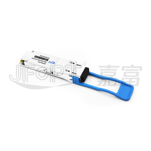
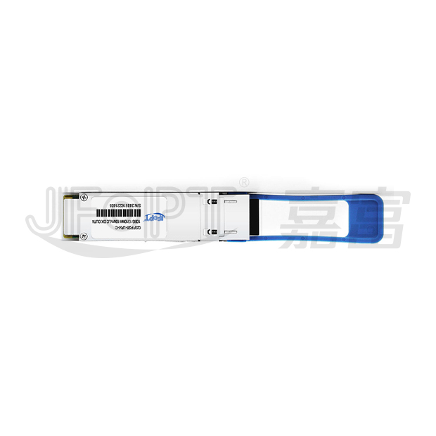
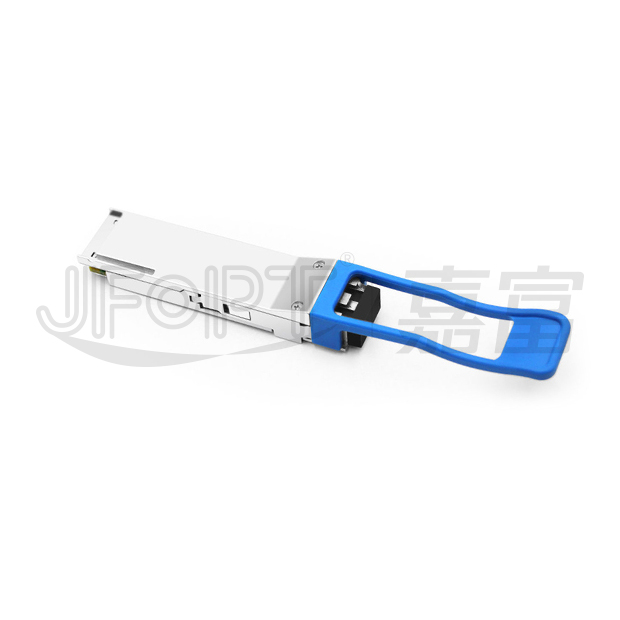
The JFOPT QSFP28 100G LAN-WDM 10km LR4 LC DX OUT4 is a 100Gb/s transceiver module designed for optical communication applications, compliant with OTU4 411-9D1F requirements as specified in ITU-T Recommendations G.959.1, G.709, and Supplement 39 (G.sup39). The module converts four 28Gb/s electrical input channels into four LAN WDM optical signals, multiplexing them into a single channel for 100Gb/s optical transmission. On the receiver side, it de-multiplexes the 100Gb/s optical input back into four LAN WDM optical signals and converts them into four electrical output channels.The central wavelengths of the four LAN WDM channels are 1295.56nm, 1300.05nm, 1304.58nm, and 1309.14nm, in accordance with the LAN WDM wavelength grid defined in IEEE 802.3ba. Equipped with high-performance cooled LAN WDM DFB transmitters and high-sensitivity PIN receivers, the module ensures exceptional performance.Designed according to the QSFP+ Multi-Source Agreement (MSA), this transceiver features a compact form factor, robust optical and electrical connections, and a digital diagnostic interface. It is engineered to operate reliably under harsh conditions, including extreme temperatures, high humidity, and EMI interference, making it ideal for demanding environments.
| Supports 112Gbps | I2C interface with integrated digital diagnostic monitoring | ||||||||
| 4*28Gbps DFB-based LAN-WDM transmitter | PIN and TIA array on the receiver side | ||||||||
| 4x28G electrical interface | Single 3.3V power supply and power dissipation<4W | ||||||||
| Distance up to 10km over SMF | Duplex LC receptacles | ||||||||
| Operating case temperature:0℃~+70℃ |
| OTU4411-9D1F | ||||||||

| Parameter | Symbol | Min. | Max. | Unit | |||||
| Supply voltage | VCC | -0.5 | +3.6 | V | |||||
| Storage temperature | TC | -40 | +85 | ℃ | |||||
| Relative humidity | RH | 5 | 85 | % | |||||
These values represent the damage threshold of the module.Stress in excess of any of the individual absolute maximum ratingscan cause immediate catastrophic damage to the module even if all other parameters are within recommended operating conditions.
| Parameter | Symbol | Min | Typical | Max | Unit | ||||
| Power supply voltage | VCC | 3.15 | 3.30 | 3.45 | V | ||||
| Operating case temperature | Tca | 0 | - | 70 | ℃ | ||||
| Parameter | Symbol | Min | Typical | Max | Unit | Ref | |||
Transmitter |
|||||||||
| Input differential impedance | Rin | - | 100 | - | Ω | 1 | |||
| Single-ended input voltage tolerance | - | -0.3 | - | 4.0 | V | - | |||
| AC common mode input voltage tolerance | - | 15 | - | - | mV | - | |||
| Differential input voltage | - | 50 | - | - | mV | - | |||
| Differential input voltage swing,per lane | Vin | 190 | - | 1000 | mV | - | |||
Receiver |
|||||||||
| Output differential impedance | Rout | - | 100 | - | Ω | 1 | |||
| Differential output swing,per lane | Vout | 300 | - | 900 | mV | 2 | |||
| AC common mode output voltage tolerance | - | - | - | 7.5 | mV | - | |||
| Single-ended output voltage | - | -0.3 | - | 4.0 | V | - | |||
Notes: [1]AC coupled. [2]Into 100 ohm differentialter mination. |
|||||||||
| Parameter | Symbol | Min | Typical | Max | Unit | Ref. | |||
| Bit rate per lane | DR | 27.9525±20ppm | Gb/s | 1 | |||||
| Data rate variation | - | -20 | - | 20 | ppm | - | |||
| Lane_0 center wavelength | λ0 | 1294.53 | 1295.56 | 1296.59 | nm | - | |||
| Lane_1 center wavelength | λ1 | 1299.02 | 1300.05 | 1301.09 | nm | - | |||
| Lane_2 center wavelength | λ2 | 1303.54 | 1304.58 | 1305.63 | nm | - | |||
| Lane_3 center wavelength | λ3 | 1308.09 | 1309.14 | 1310.19 | nm | - | |||
| Total average output power | Po | - | - | 10.5 | dBm | - | |||
| Average launch power each lane | - | -0.6 | - | 4 | dBm | 2,6 | |||
| Difference in launch power between any two lanes(OMA) | - | - | - | 5 | dB | - | |||
| Extinction ratio | ER | 4 | - | - | dB | - | |||
| Side-mode suppression ratio | SMSR | 30 | - | - | dB | - | |||
| Average launch power of OFF transmitterper lane | Poff | - | - | -30 | dBm | - | |||
| Transmitter reflectance | - | - | - | -12 | dB | - | |||
| Optical return loss tolerance | ORL | - | - | 20 | dB | - | |||
| Transmitter eye mask definition{X1,X2,X3,Y1,Y2,Y3} | {0.25,0.4,0.45,0.25,0.28,0.4} | 3 | |||||||
| Parameter | Symbol | Min. | Typical | Max. | Unit | Ref. | |||
| Bit rate per channel | DR | 27.9525±20ppm | Gb/s | 4 | |||||
| Data rate variation | - | -20 | - | 20 | ppm | - | |||
| Lane_0 center wavelength | λ0 | 1294.53 | 1295.56 | 1296.59 | nm | - | |||
| Lane_1 center wavelength | λ1 | 1299.02 | 1300.05 | 1301.09 | nm | - | |||
| Lane_2 center wavelength | 入2 | 1303.54 | 1304.58 | 1305.63 | nm | - | |||
| Lane_3 center wavelength | λ3 | 1308.09 | 1309.14 | 1310.19 | nm | - | |||
| Average receive power per lane | RXPOW | -6.9 | - | 4 | dBm | 5,6 | |||
| Receive sensitivity in OMA per lane | Rsen | - | - | -8.4 | dBm | - | |||
| Optical return loss | ORL | - | - | -26 | dB | - | |||
| LOS assert | Lsa | -25 | - | - | dBm | - | |||
| LOS DE-assert | Lda | - | - | -12 | dBm | - | |||
| LOS hysteresis | Lh | 0.5 | - | - | dB | - | |||
Notes: [1]Transmitter consists of 4lasers operating at 27.95Gb/s each. [2]Minimum value is informative. [3]Hit ratio 5x10⁻⁵. [4]Receiver consists of4 photodetectors operatingat 27.95Gb/s each. [5]Minimum value is informative,equals min TxOMA with infinite ER and max channel insertion loss. [6]Power value and power accuracy are with allchannels on. |
|||||||||
| Parameter | Symbol | Min. | Typical | Max. | Unit | Ref. | |||
| Bit rate(all wavelengths combined) | BR | - | - | 112 | Gb/s | 1 | |||
| Bit error ratio @25.78Gb/s | BER | - | - | 10-6 | - | 2 | |||
Maximum supported distances |
|||||||||
| Fiber type | - | - | - | - | - | - | |||
| SMF per G.652 | Lmax | - | - | 10 | km | - | |||
Notes: [1]Supports OTU4411-9D1F per ITU-T G.959.1. [2]Tested with a 231-1PRBS. |
|||||||||
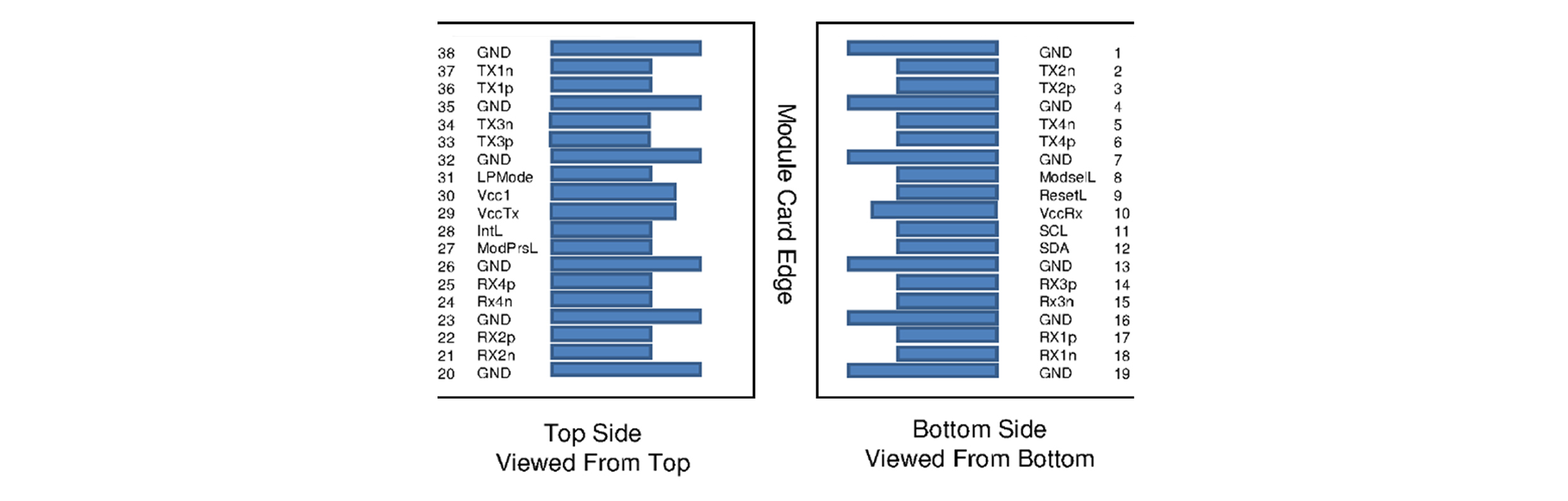
| Pin | Symbol | Name/Description | |||||||
| 1 | GND | Ground | |||||||
| 2 | Tx2n | Transmitter inverted data input | |||||||
| 3 | Tx2p | Transmitter non-inverted data input | |||||||
| 4 | GND | Ground | |||||||
| 5 | Tx4n | Transmitter inverted data input | |||||||
| 6 | Tx4p | Transmitter non-inverted data input | |||||||
| 7 | GND | Ground | |||||||
| 8 | ModSelL | Module select | |||||||
| 9 | ResetL | Module reset | |||||||
| 10 | VCCRx | +3.3V power supply receiver | |||||||
| 11 | SCL | 2-wire serial interface clock | |||||||
| 12 | SDA | 2-wire serial interface data | |||||||
| 13 | GND | Ground | |||||||
| 14 | Rx3p | Receiver non-inverted data output | |||||||
| 15 | Rx3n | Receiver inverted data output | |||||||
| 16 | GND | Ground | |||||||
| 17 | Rxlp | Receiver non-inverted data output | |||||||
| 18 | Rx1n | Receiver inverted data output | |||||||
| 19 | GND | Ground | |||||||
| 20 | GND | Ground | |||||||
| 21 | Rx2n | Receiver inverted data output | |||||||
| 22 | Rx2p | Receiver non-inverted data output | |||||||
| 23 | GND | Ground | |||||||
| 24 | Rx4n | Receiver inverted data output | |||||||
| 25 | Rx4p | Receiver non-inverted data output | |||||||
| 26 | GND | Ground | |||||||
| 27 | ModPrsL | Module present | |||||||
| 28 | IntL | Interrupt | |||||||
| 29 | VCC Tx | +3.3V power supply transmitter | |||||||
| 30 | VCC1 | +3.3V power Supply | |||||||
| 31 | LPMode | Low power mode | |||||||
| 32 | GND | Ground | |||||||
| 33 | Tx3p | Transmitter non-inverted data input | |||||||
| 34 | Tx3n | Transmitter inverted data input | |||||||
| 35 | GND | Ground | |||||||
| 36 | Txlp | Transmitter non-inverted dataInput | |||||||
| 37 | Tx1n | Transmitter inverted data input | |||||||
| 38 | GND | Ground | |||||||


 Ann
Ann


