


|
Product model
|
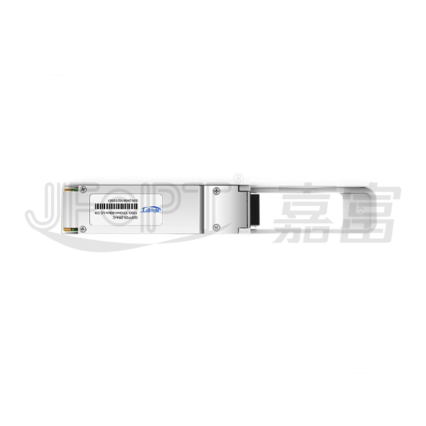
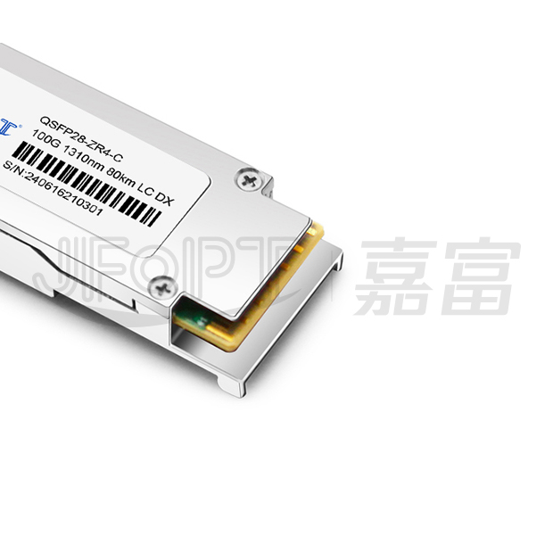
JFTSM-QSFP28-100-LW-80(ZR4)-LCD
|
Manufacturer brand
|
JFOPT
|
|
Package type
|
QSFP28
|
Optical connector
|
LC DX
|
|
Max data rate
|
111.81Gbps
|
Channel data rate
|
25.78125Gbps
|
|
Effective transmission distance
|
80km
|
||
|
Wavelength
|
1310nm
|
Operating voltage
|
3.3V
|
|
Fiber type
|
SMF
|
Core size
|
9/125
|
|
Transmitter type
|
LAN WDM EML
|
Receiver type
|
PIN
|
|
TX power
|
2.0~6dBm
|
Receiver sensitivity
|
-28Bm
|
|
Digital optical monitoring(DDM)
|
YES
|
Receiver overload
|
4.5dBm
|
|
Power consumption
|
<6.5W
|
Protocols
|
100GBASE-ZR4
Ethernet Links |
|
Operating temperature(Commercial)
|
0℃~+70℃
|
Storage temperature(Commercial)
|
-40℃~+85℃
|
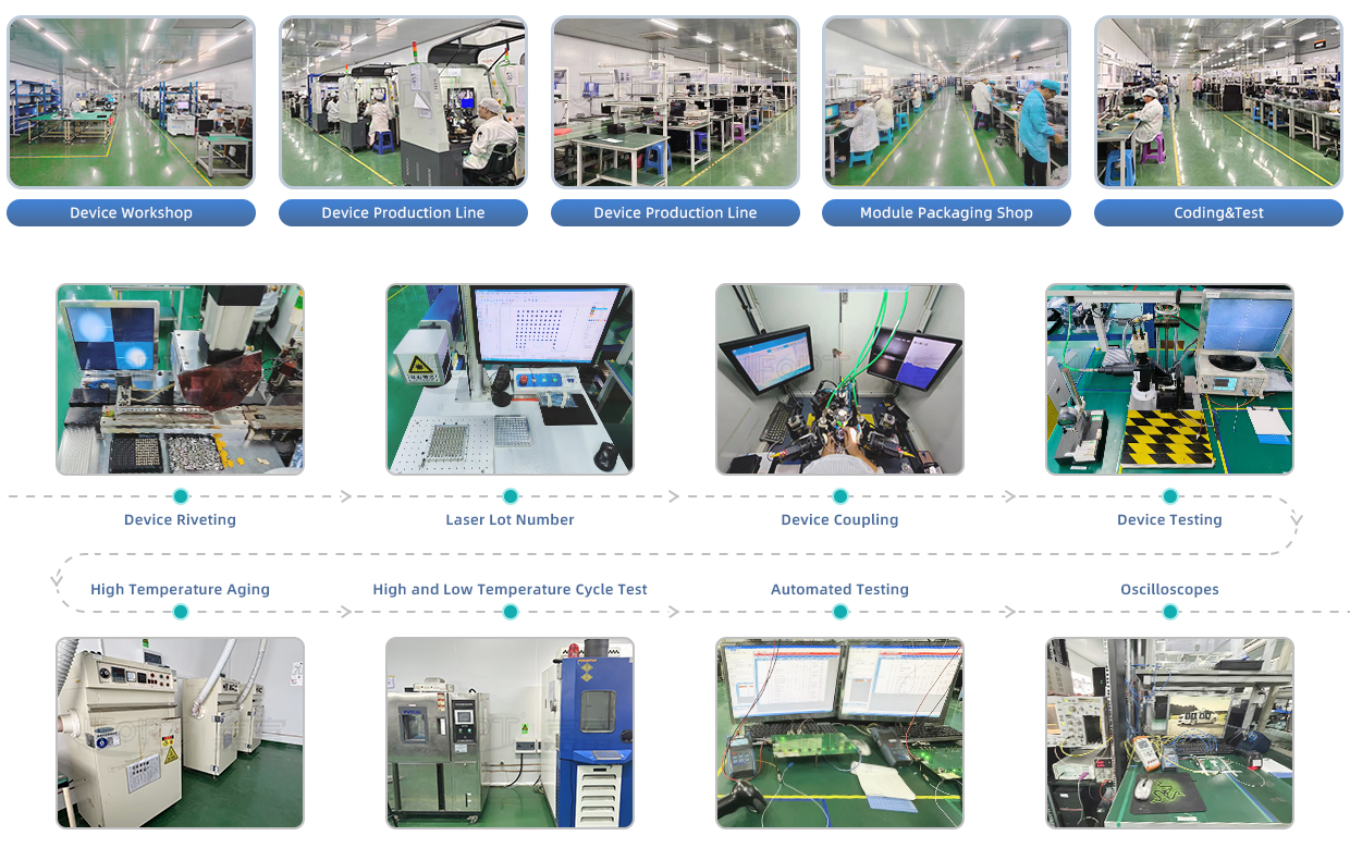
JFOPT continues to invest in optical transceiver production, covering a full range of optical transceiver such as 1*9, SFP, 10G, 25G, 100G, 200G, 400G, 800G GPON/EPON/XG/XGSPON OLT transceiver. At the same time, our company provides TOSA, ROSA, BOSA semi-finished device solutions for the downstream peer. JFOPT's production line has a daily production capacity of 10,000 optical transceivers and 20,000 optical devices. In addition, JFOPT's optical transceiver have industry-leading high temperature resistance and anti-interference capability, and are widely used in computing centers, operators, traffic security, power facilities and other industries.
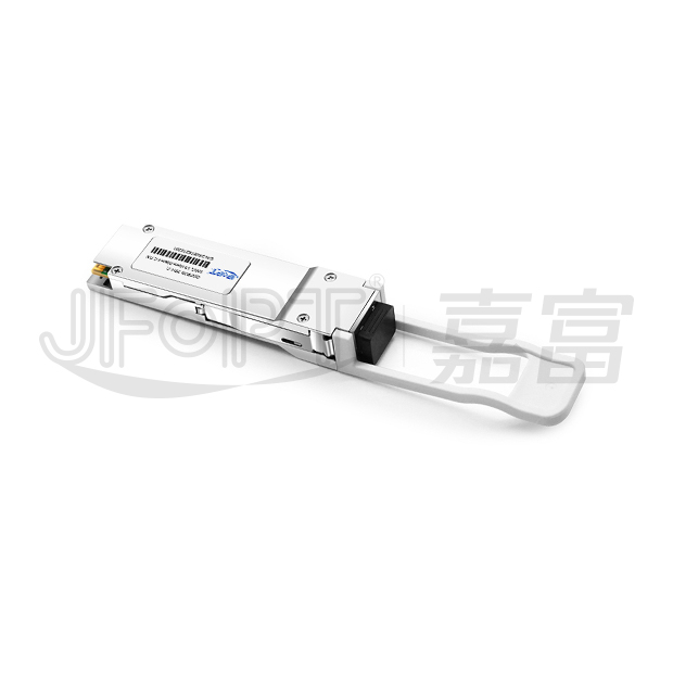
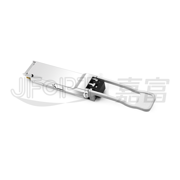
The JFOPT QSFP28 100G LAN-WDM 80km LC DX Transceiver is a high-performance module designed for 80km optical communication applications. It integrates a 4-lane optical transmitter, a 4-lane optical receiver, and a module management block with a 2-wire serial interface. The optical signals are multiplexed onto a single-mode fiber via an industry-standard LC connector.Built in compliance with the QSFP+ Multi-Source Agreement (MSA), the transceiver features a compact form factor, robust optical/electrical connections, and a digital diagnostic interface. It is engineered to withstand harsh external conditions, including extreme temperatures, high humidity, and EMI interference, ensuring reliable performance in demanding environments.
| Compliant with 100GBASE-ZR4 | Support line rates from 103.125Gb/s to 111.81Gb/s OTU4 | |||||||
| LAN WDM EML laser and PIN receiver with SOA | Up to 80km reach for G.652 SMF | |||||||
| Hot pluggable 38 pin electrical interface | QSFP28 MSA compliant | |||||||
| Duplex LC optical receptacle | Maximum power consumption 6.5W | |||||||
| Single+3.3V power supply | Case operating temperature:0~+70℃ | |||||||
| 100GBASE-LR4 100G ethernet | ||||||||

| Parameter | Symbol | Min. | Max. | Unit | |||||
| Supply voltage | VCC | -0.5 | +3.6 | V | |||||
| Storage temperature | TC | -40 | +85 | ℃ | |||||
| Relative humidity | RH | 5 | 85 | % | |||||
These values represent the damage threshold of the module.Stress in excess of any of the individual absolute maximum ratingscan cause immediate catastrophic damage to the module even if all other parameters are within recommended operating conditions.
| Parameter | Symbol | Min | Typical | Max | Unit | ||||
| Power supply voltage | VCC | 3.15 | 3.3 | 3.45 | V | ||||
| Operating case temperature | Tca | 0 | - | 70 | ℃ | ||||
| Link distance | D | - | - | 80 | km | ||||
| Parameter | Symbol | Min | Typical | Max | Unit | Ref | |||
Transmitter |
|||||||||
| Input differential impedance | Rin | 90 | 100 | 110 | Ω | 1 | |||
| Differential input voltage amplitude | Vin | - | - | 900 | mVp-p | 2 | |||
Receiver |
|||||||||
| Output differential impedance | Rout | 90 | 100 | 110 | Ω | 1 | |||
| Differential output voltage amplitude |
Vout | 300 | - | 900 | mVp-p | 3 | |||
Notes: [1]AC coupled. [2]Differential input voltage amplitude is measured between TxnP and TxnN. [3]Differentialoutput voltage amplitude is measured between RxnP and RxnN. |
|||||||||
| Parameter | Symbol | Min | Typical | Max | Unit | ||||
| Center wavelength | Ch0 | λ0 | 1294.53 | 1295.56 | 1296.59 | nm | |||
| Ch1 | λ1 | 1299.02 | 1300.05 | 1301.09 | nm | ||||
| Ch2 | λ2 | 1303.54 | 1304.58 | 1305.63 | nm | ||||
| Ch3 | λ3 | 1308.09 | 1309.14 | 1310.09 | nm | ||||
| Bit rate per channel | B | 25.78125±100ppm | Gbps | ||||||
| Side mode suppression ratio | SMSR | 30 | - | - | dB | ||||
| Average launch power,each lane | - | 2 | - | 6 | dBm | ||||
| Launch power in OMA minus TDP,each lane | OMA-TDP | -0.7 | - | - | dBm | ||||
| Transmission & dispersion penalty, each lane | TDP | - | - | 2.5 | |||||
| Relative intensity noise | RIN | - | - | -130 | dB/Hz | ||||
| Transmitter reflectance | - | - | - | -20.0 | dB | ||||
| Extinction ratio | ER | 6 | - | - | dB | ||||
| Transmitter eye mask definition {X1,X2,X3,Y1,Y2,Y3} | {0.25,0.4,0.45,0.25,0.28,0.4} | ||||||||
| Average launch power of OFF transmitter,each lane | - | - | - | -30 | dBm | ||||
| Optical return loss tolerance | - | - | - | 20 | dB | ||||
| Parameter | Symbol | Min. | Typical | Max. | Unit | ||||
| Center wavelength | Ch0 | λ0 | 1294.53 | 1295.56 | 1296.59 | nm | |||
| Ch1 | λ1 | 1299.02 | 1300.05 | 1301.09 | nm | ||||
| Ch2 | λ2 | 1303.54 | 1304.58 | 1305.63 | nm | ||||
| Ch3 | λ3 | 1308.09 | 1309.14 | 1310.09 | nm | ||||
| Bit rateper channel | B | 25.78125±100ppm | Gbps | ||||||
| Damage threshold,each lane | - | 6.5 | - | - | dBm | ||||
| Average receive power,each lane | - | -28.0 | - | -7 | dbm | ||||
| Unstressed sensitivity (OMA) at 5x10⁻⁵ BER | OMAin | - | - | -28 | dBm | ||||
| LOS assert | LOSA | -40 | - | - | dBm | ||||
| LOS de-assert | LOSD | - | - | -29 | dBm | ||||
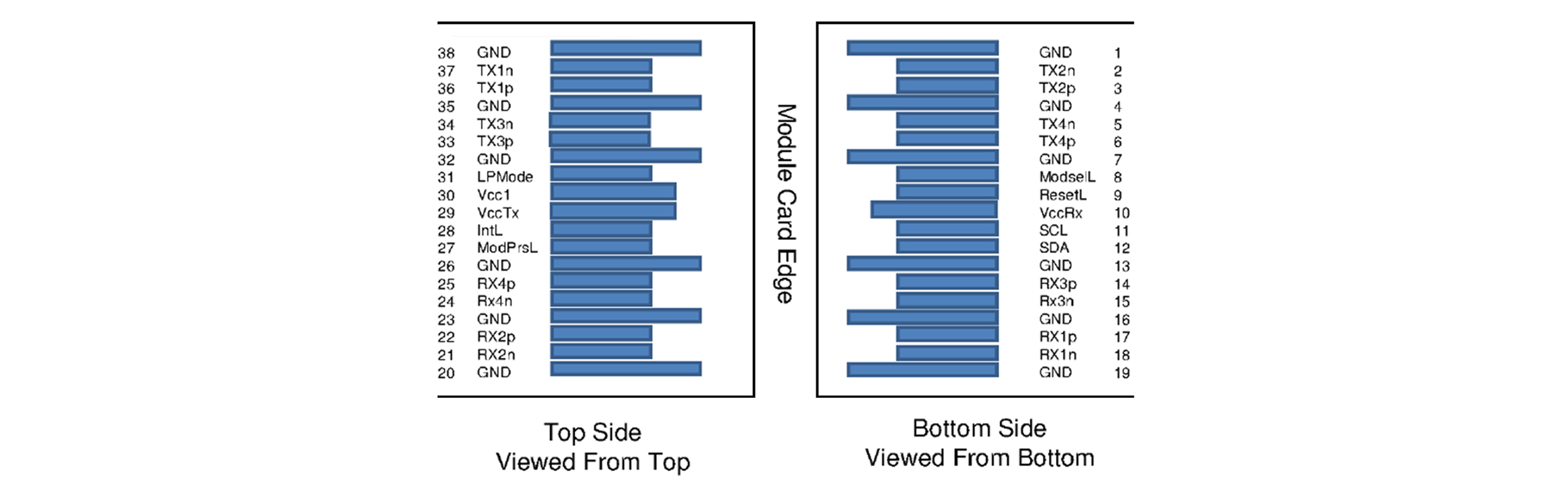
| Pin | Symbol | Name/Description | |||||||
| 1 | GND | Ground | |||||||
| 2 | Tx2n | Transmitter inverted data input | |||||||
| 3 | Tx2p | Transmitter non-inverted data input | |||||||
| 4 | GND | Ground | |||||||
| 5 | Tx4n | Transmitter inverted data input | |||||||
| 6 | Tx4p | Transmitter non-inverted data input | |||||||
| 7 | GND | Ground | |||||||
| 8 | ModSelL | Module select | |||||||
| 9 | ResetL | Module reset | |||||||
| 10 | VCCRx | +3.3V power supply receiver | |||||||
| 11 | SCL | 2-wire serial interface clock | |||||||
| 12 | SDA | 2-wire serial interface data | |||||||
| 13 | GND | Ground | |||||||
| 14 | Rx3p | Receiver non-inverted data output | |||||||
| 15 | Rx3n | Receiver inverted data output | |||||||
| 16 | GND | Ground | |||||||
| 17 | Rxlp | Receiver non-inverted data output | |||||||
| 18 | Rx1n | Receiver inverted data output | |||||||
| 19 | GND | Ground | |||||||
| 20 | GND | Ground | |||||||
| 21 | Rx2n | Receiver inverted data output | |||||||
| 22 | Rx2p | Receiver non-inverted data output | |||||||
| 23 | GND | Ground | |||||||
| 24 | Rx4n | Receiver inverted data output | |||||||
| 25 | Rx4p | Receiver non-inverted data output | |||||||
| 26 | GND | Ground | |||||||
| 27 | ModPrsL | Module present | |||||||
| 28 | IntL | Interrupt | |||||||
| 29 | VCC Tx | +3.3V power supply transmitter | |||||||
| 30 | VCC1 | +3.3V power Supply | |||||||
| 31 | LPMode | Low power mode | |||||||
| 32 | GND | Ground | |||||||
| 33 | Tx3p | Transmitter non-inverted data input | |||||||
| 34 | Tx3n | Transmitter inverted data input | |||||||
| 35 | GND | Ground | |||||||
| 36 | Txlp | Transmitter non-inverted dataInput | |||||||
| 37 | Tx1n | Transmitter inverted data input | |||||||
| 38 | GND | Ground | |||||||


 Ann
Ann


