


|
Product model
|
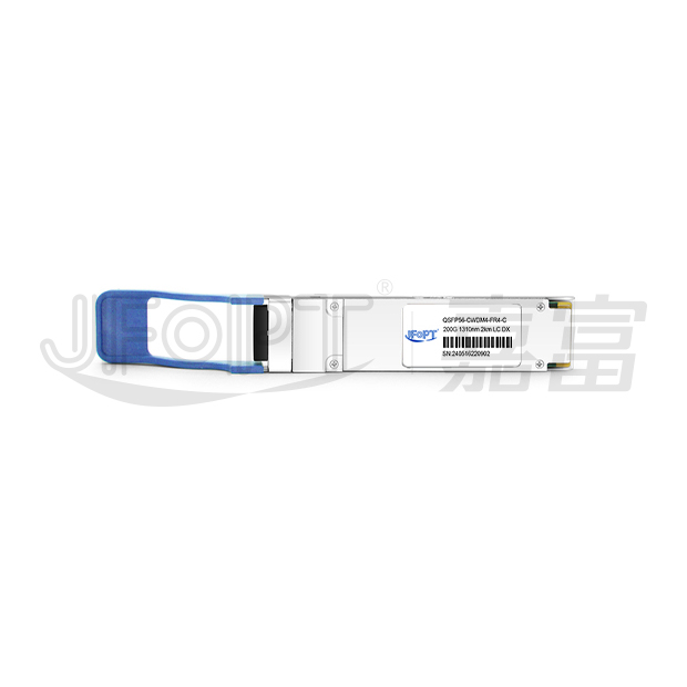
JFTSM-QSFP56-200(4x50)-CW4-2(FR4)-LCD
|
Manufacturer brand
|
JFOPT
|
|
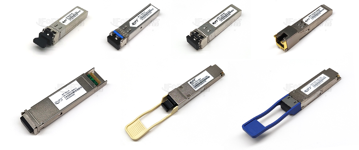
Package type
|
QSFP56
|
Optical connector
|
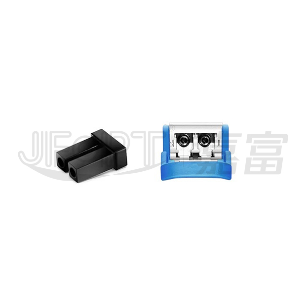
LC DX
|
|
Max data rate
|
200Gbps
|
Channel data rate
|
26.5625Gbps
|
|
Effective transmission distance
|
2km
|
||
|
Wavelength
|
1310nm
|
Operating voltage
|
3.3V
|
|
Fiber type
|
SMF
|
Core size
|
9/125
|
|
Transmitter type
|
CWDM LD&PD
|
Receiver type
|
PIN
|
|
TX power
|
-4.2~4.7dBm
|
Receiver sensitivity
|
-6dBm
|
|
Digital optical monitoring(DDM)
|
YES
|
Receiver overload
|
4.7dBm
|
|
Power consumption
|
<6.5W
|
Protocols
|
200G BASE-FR4 ethernet
Switch & Router Connections Data center Other 200G interconnect requirements |
|
Operating temperature(Commercial)
|
0℃~+70℃
|
Storage temperature(Commercial)
|
-40℃~+85℃
|
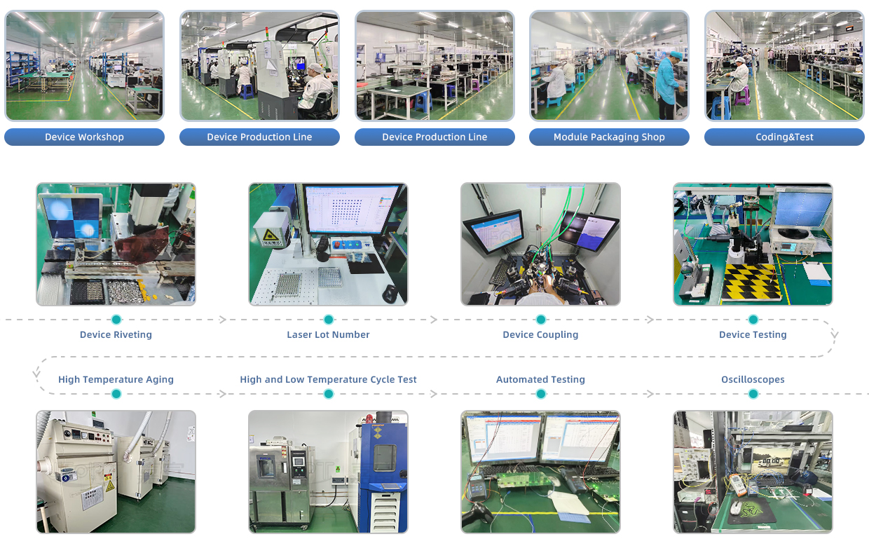
JFOPT continues to invest in optical transceiver production, covering a full range of optical transceiver such as 1*9, SFP, 10G, 25G, 100G, 200G, 400G, 800G GPON/EPON/XG/XGSPON OLT transceiver. At the same time, our company provides TOSA, ROSA, BOSA semi-finished device solutions for the downstream peer. JFOPT's production line has a daily production capacity of 10,000 optical transceivers and 20,000 optical devices. In addition, JFOPT's optical transceiver have industry-leading high temperature resistance and anti-interference capability, and are widely used in computing centers, operators, traffic security, power facilities and other industries.
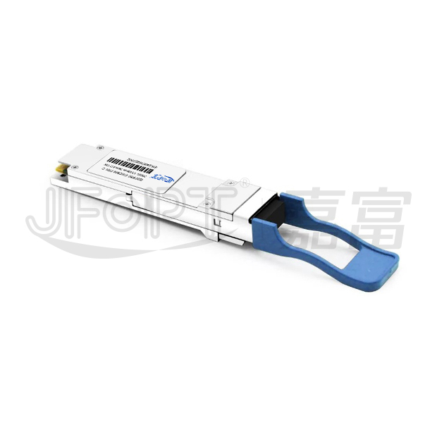
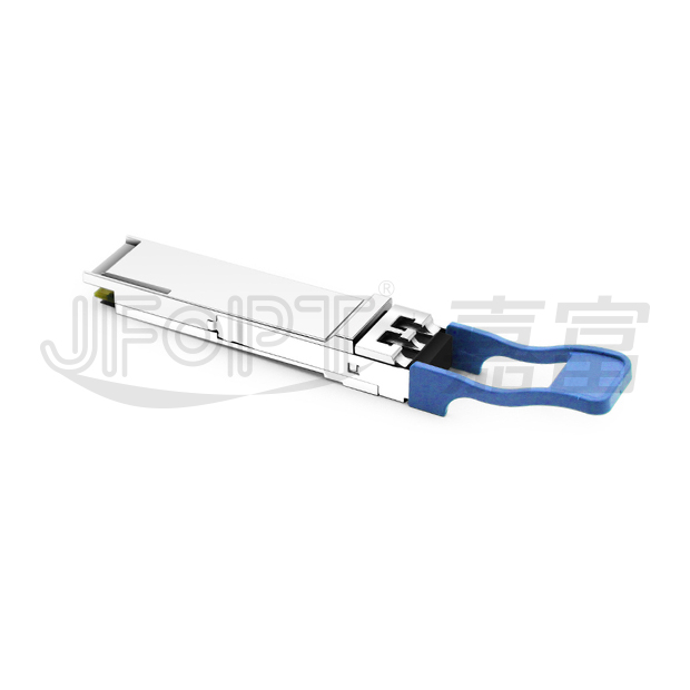
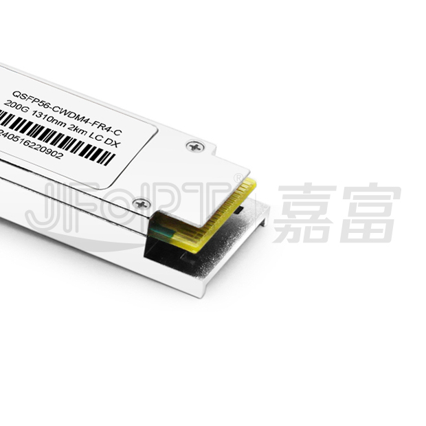
The JFOPT QSFP56 200G (4x50G) CWDM4 2km FR4 LC DX Transceiver is a high-performance, hot-pluggable module designed for optical data transmission at 50Gbps per channel using PAM4 modulation. It supports data links over single-mode fiber at distances of up to 2km and is housed in a compact QSFP56 package. The transceiver integrates advanced components, including a high-performance laser diode (LD), photodetector (PIN), and digital signal processor (DSP), ensuring reliable and efficient operation for demanding data communication applications.
| Hot-pluggable QSFP56 form factor | LC/UPC connecting interface compliant | ||||||||
| Data rate up to 50 Gb/s PAM4 per lane | Integrated CWDM LD and PD array | ||||||||
| Maximum link length of 2km via SMF fiber | Digital diagnostics functions are available via the I2C interface | ||||||||
| Single 3.3V power supply | Power dissipation:<6.5W | ||||||||
| International class 1 laser safety certified | Operating case temperature:0℃~+70℃ |
| 200G BASE-FR4 ethernet | Switch & Router connections | |||||||
| Data centers | Other 200G interconnect requirements | |||||||

| Parameter | Symbol | Min. | Max. | Unit | |||||
| Power supply voltage | VCC | -0.5 | +3.6 | V | |||||
| Storage temperature | TC | -40 | +85 | ℃ | |||||
| Relative humidity | RH | 5 | 85 | % | |||||
These values represent the damage threshold of the module.Stress in excess of any of the individual absolute maximum ratingscan cause immediate catastrophic damage to the module even if all other parameters are within recommended operating conditions.
| Parameter | Symbol | Min | Typical | Max | Unit | ||||
| Power supply voltage | VCC | 3.135 | 3.30 | 3.465 | V | ||||
| Operating case temperature | Tca | 0 | - | 70 | ℃ | ||||
Recommended operating environment specifies parameters for which the electrical and optical characteristics hold unless otherwise noted.
| Parameter | Symbol | Min | Typical | Max | Unit | Notes | |||
| Signaling rate per lane | - | - | 26.5625 | - | Gbd | - | |||
Transmitter |
|||||||||
| Differential data input voltage | △Vin | 900 | - | - | mVp-p | - | |||
| DifferentialInput Impedance | Zin | 90 | 100 | 110 | ohm | - | |||
Receiver |
|||||||||
| Differential output voltage | Vout | - | - | 900 | mVp-p | - | |||
| Differential output impedance | Rout | 90 | 100 | 110 | ohm | - | |||
| Parameter | Symbol | Min | Typical | Max | Unit | Notes | |||
Transmitter |
|||||||||
| Center wavelength | Ch0 | λ0 | 1264.5 | 1271 | 1277.5 | nm | - | ||
| Ch1 | λ1 | 1284.5 | 1291 | 1297.5 | |||||
| Ch2 | λ2 | 1304.5 | 1311 | 1317.5 | |||||
| Ch3 | λ3 | 1324.5 | 1331 | 1337.5 | |||||
| Side-mode suppression ratio | SMSR | 30 | - | - | dB | - | |||
| Average optical power | Po | -4.2 | - | 4.7 | dBm | - | |||
| Tx OMA per lane | TxOMA | -1.2 | - | 4.5 | dBm | - | |||
| Extinction ratio | ER | 3.5 | - | - | dBm | - | |||
| Optical modulation amplitude | OMA | -4.5 | - | 3 | dB | - | |||
| Transmitter and dispersion eye closure for PAM4 per lane | TDECQ | - | - | 3.3 | dB | - | |||
| Optical return loss tolerance | ORL | - | - | 16.5 | dB | - | |||
| Relative intensity noise | RIN | - | - | -132 | dB/Hz | - | |||
Receiver |
|||||||||
| Center wavelength | Ch0 | λ0 | 1264.5 | 1271 | 1277.5 | nm | |||
| Ch1 | λ1 | 1284.5 | 1291 | 1297.5 | |||||
| Ch2 | λ2 | 1304.5 | 1311 | 1317.5 | |||||
| Ch3 | λ3 | 1324.5 | 1331 | 1337.5 | |||||
| Damage threshold | DT | 5.7 | - | - | dBm | - | |||
| Average receive power ,each lane | - | -8.2 | - | 4.7 | dBm | - | |||
| Receiver reflectance | Rfl | - | - | -26 | dB | - | |||
| Difference in receive power between any two lanes | - | - | - | 4.1 | dB | - | |||
| Receiver sensitivity(OMAouter) | - | - | - | -6 | dBm | - | |||
| Stressed receiver sensitivity(OMAouter) | - | - | - | -3.6 | dBm | - | |||
The following optical characteristics are defined over the recommended operating environment unless otherwise specified.
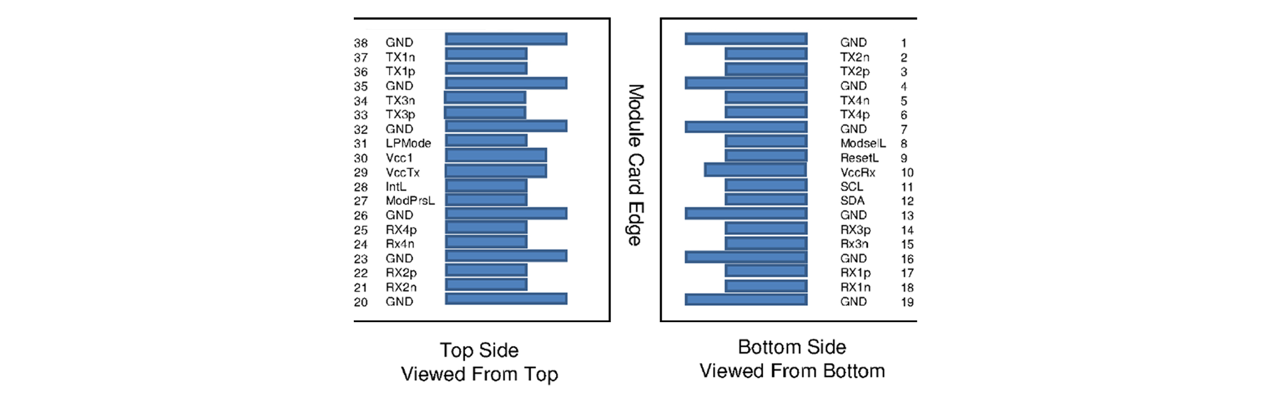
| Pin | Symbol | Name/Description | |||||||
| 1 | GND | Ground | |||||||
| 2 | Tx2n | Transmitter inverted data input | |||||||
| 3 | Tx2p | Transmitter non-inverted data input | |||||||
| 4 | GND | Ground | |||||||
| 5 | Tx4n | Transmitter inverted data input | |||||||
| 6 | Tx4p | Transmitter non-inverted data input | |||||||
| 7 | GND | Ground | |||||||
| 8 | ModSelL | Module select | |||||||
| 9 | ResetL | Module reset | |||||||
| 10 | VCCRx | +3.3V power supply receiver | |||||||
| 11 | SCL | 2-wire serial interface clock | |||||||
| 12 | SDA | 2-wire serial interface data | |||||||
| 13 | GND | Ground | |||||||
| 14 | Rx3p | Receiver non-inverted data output | |||||||
| 15 | Rx3n | Receiver inverted data output | |||||||
| 16 | GND | Ground | |||||||
| 17 | Rxlp | Receiver non-inverted data output | |||||||
| 18 | Rx1n | Receiver inverted data output | |||||||
| 19 | GND | Ground | |||||||
| 20 | GND | Ground | |||||||
| 21 | Rx2n | Receiver inverted data output | |||||||
| 22 | Rx2p | Receiver non-inverted data output | |||||||
| 23 | GND | Ground | |||||||
| 24 | Rx4n | Receiver inverted data output | |||||||
| 25 | Rx4p | Receiver non-inverted data output | |||||||
| 26 | GND | Ground | |||||||
| 27 | ModPrsL | Module present | |||||||
| 28 | IntL | Interrupt | |||||||
| 29 | VCC Tx | +3.3V power supply transmitter | |||||||
| 30 | VCC1 | +3.3V power Supply | |||||||
| 31 | LPMode | Low power mode | |||||||
| 32 | GND | Ground | |||||||
| 33 | Tx3p | Transmitter non-inverted data input | |||||||
| 34 | Tx3n | Transmitter inverted data input | |||||||
| 35 | GND | Ground | |||||||
| 36 | Txlp | Transmitter non-inverted dataInput | |||||||
| 37 | Tx1n | Transmitter inverted data input | |||||||
| 38 | GND | Ground | |||||||


 Ann
Ann


