


|
Product model
|
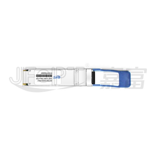
JFTSM-QSFP56-200(4x50)-CW4-10(LR4)-LCD
|
Manufacturer brand
|
JFOPT
|
|
Package type
|
QSFP56
|
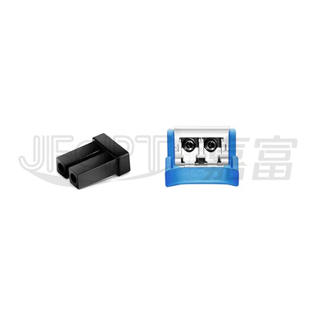
Optical connector
|
LC DX
|
|
Max data rate
|
200Gbps
|
Channel data rate
|
26.5625Gbps
|
|
Effective transmission distance
|
10km
|
||
|
Wavelength
|
1310nm
|
Operating voltage
|
3.3V
|
|
Fiber type
|
SMF
|
Core size
|
9/125
|
|
Transmitter type
|
DFB
|
Receiver type
|
PIN
|
|
TX power
|
-3.4~5.3dBm
|
Receiver sensitivity
|
-7.7dBm
|
|
Digital optical monitoring(DDM)
|
YES
|
Receiver overload
|
5.3dBm
|
|
Power consumption
|
<8W
|
Protocols
|
5G backhaul
Switch&Router connections Data centers 200GE 10km SMF links |
|
Operating temperature(Commercial)
|
0℃~+70℃
|
Storage temperature(Commercial)
|
-40℃~+85℃
|
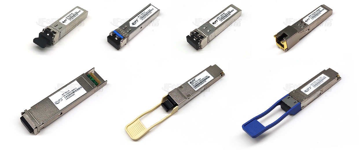
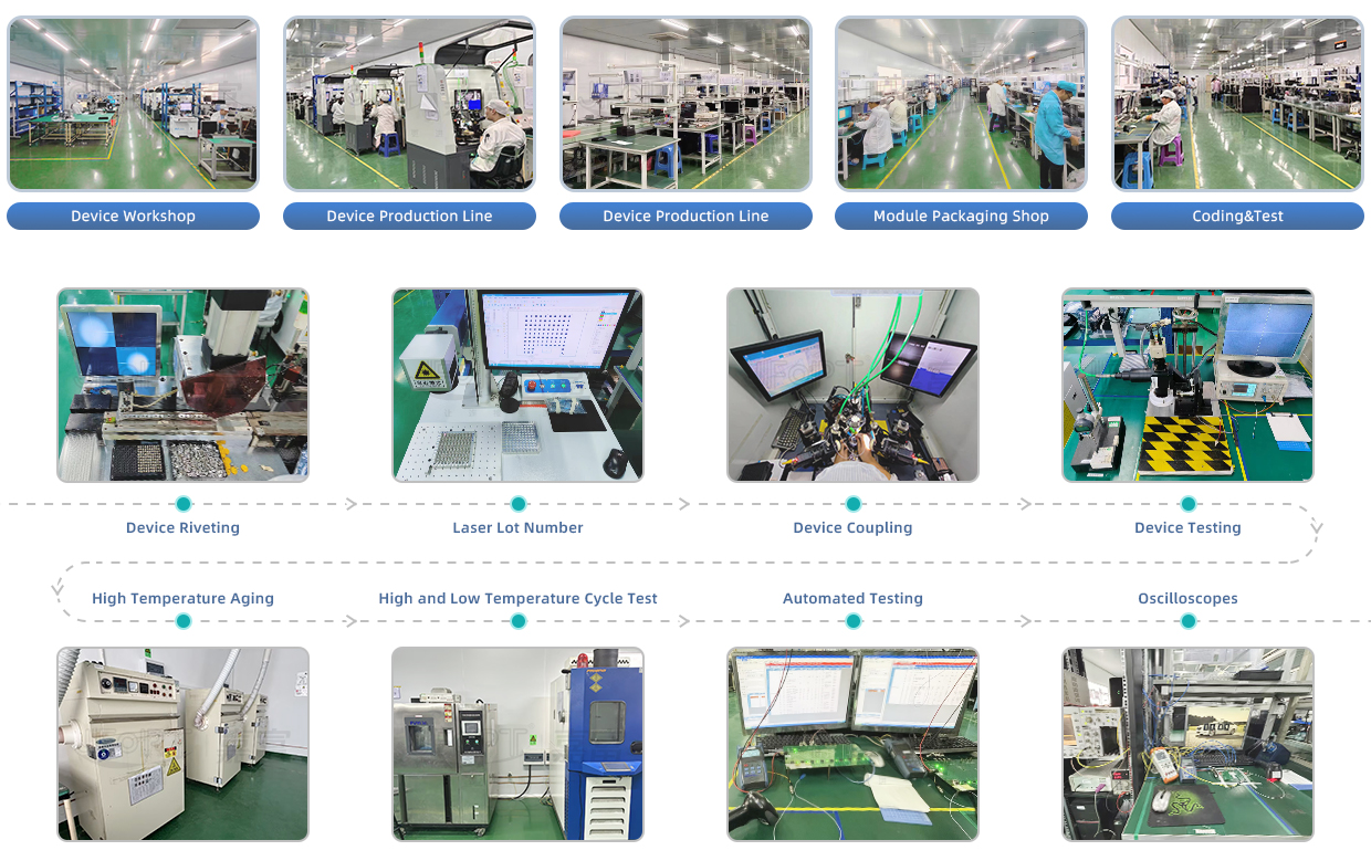
JFOPT continues to invest in optical transceiver production, covering a full range of optical transceiver such as 1*9, SFP, 10G, 25G, 100G, 200G, 400G, 800G GPON/EPON/XG/XGSPON OLT transceiver. At the same time, our company provides TOSA, ROSA, BOSA semi-finished device solutions for the downstream peer. JFOPT's production line has a daily production capacity of 10,000 optical transceivers and 20,000 optical devices. In addition, JFOPT's optical transceiver have industry-leading high temperature resistance and anti-interference capability, and are widely used in computing centers, operators, traffic security, power facilities and other industries.
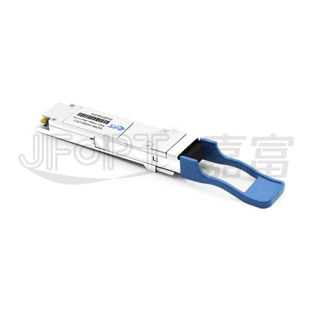
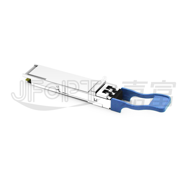
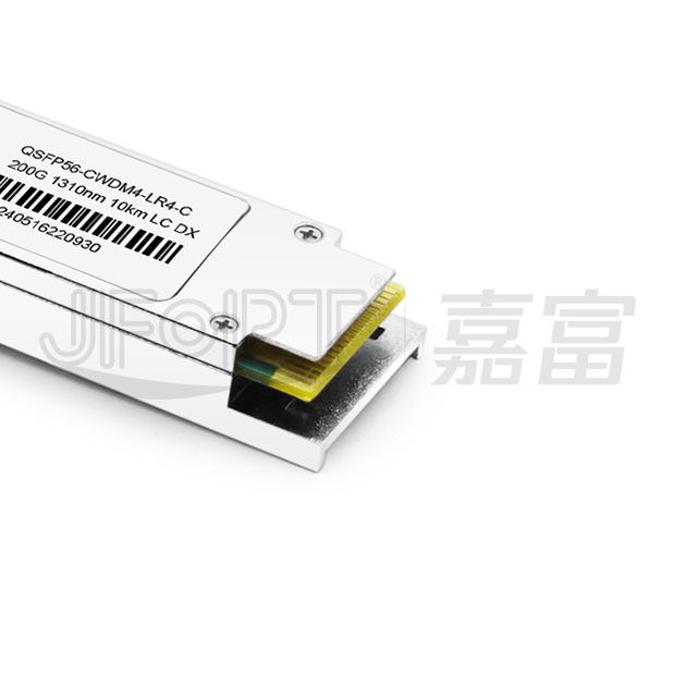
The JFOPT QSFP56 200G (4x50G) CWDM4 10km LR4 LC DX Transceiver is a high-performance, hot-pluggable optical module designed for 200GE links over single-mode fiber (SMF) at distances of up to 10km. It combines four 26.5625 GBd PAM4 electrical lanes into four corresponding optical channels, fully compliant with IEEE 200GBASE-LR4 standards. This transceiver delivers superior performance and reliability with an advanced design that incorporates cooled EA-DFB lasers at LAN-WDM 1.3μm wavelengths and four PIN photodetectors with low-power TIAs. The optical signals are multiplexed and demultiplexed onto a single fiber pair through an LC duplex connector, ensuring efficient and reliable data transmission.
| Hot-pluggable QSFP56 form factor | LC connector | ||||||||
| 200GBASE-LR4 compliant-4x26.5625 GBd PAM4 | 200GAUI-4 compliant-4x26.5625 GBd PAM4 | ||||||||
| Maximum link length of 10km via SMF fiber | Digital diagnostics functions are available via the I2C interface | ||||||||
| Single 3.3V power supply | Power dissipation:<8W | ||||||||
| CMIS 4.0 management interface | Operating case temperature:0℃~+70℃ |
| 5G backhaul | Switch & Router connections | |||||||
| Data centers 200GE 10Km SMF links | ||||||||

| Parameter | Symbol | Min. | Max. | Unit | |||||
| Power supply voltage | VCC | -0.5 | +3.6 | V | |||||
| Storage temperature | TC | -40 | +85 | ℃ | |||||
| Relative humidity | RH | 5 | 85 | % | |||||
These values represent the damage threshold of the module.Stress in excess of any of the individual absolute maximum ratingscan cause immediate catastrophic damage to the module even if all other parameters are within recommended operating conditions.
| Parameter | Symbol | Min | Typical | Max | Unit | ||||
| Power supply voltage | VCC | 3.135 | 3.30 | 3.465 | V | ||||
| Operating case temperature | Tca | 0 | - | 70 | ℃ | ||||
Recommended operating environment specifies parameters for which the electrical and optical characteristics hold unless otherwise noted.
| Parameter | Symbol | Min | Typical | Max | Unit | Notes | |||
| Signaling rate per lane | - | -100ppm | 26.5625 | +100ppm | Gbd | - | |||
Transmitter |
|||||||||
| Differential input impedance | Zin | 90 | 100 | 110 | ohm | - | |||
| Differential input voltage amplitude | △Vin | - | - | 900 | mVp-p | - | |||
Receiver |
|||||||||
| Differential output impedance | Zout | 90 | 100 | 110 | ohm | - | |||
| Differential output voltage amplitude | △Vout | 900 | - | - | mVp-p | AtTPla | |||
The following electrical characteristics are defined over the Recommended Operating Environment unless otherwise specified.
| Parameter | Symbol | Min | Typical | Max | Unit | Notes | |||
Transmitter |
|||||||||
| Center wavelength | Ch0 | λo | 1294.53 | - | 1296.59 | nm | - | ||
| Ch1 | λ1 | 1299.02 | - | 1301.09 | |||||
| Ch2 | λ2 | 1303.54 | - | 1305.63 | |||||
| Ch3 | λ3 | 1308.09 | - | 1310.19 | |||||
| Side-mode suppression ratio | SMSR | 30 | - | - | dB | - | |||
| Average optical power,each lane | Po | -3.4 | - | 5.3 | dBm | - | |||
| Outer optical modulation amplitude(each ane) | OMAout | -0.4 | - | 5.1 | dBm | - | |||
| Launch power in OMAouter minus TDECQ | Ptdecq | -1.8 | - | - | dBm | - | |||
| Extinction ratio | ER | 3.5 | - | - | dBm | - | |||
| Transmitter and dispersion eye closurefor PAM4 per lane | TDECQ | - | - | 3.4 | dB | - | |||
| Average launch power of off transmitter(each lane) | Poff | - | - | -30 | dBm | - | |||
| Optical return Loss tolerance | ORL | - | - | 15.1 | dB | - | |||
Receiver |
|||||||||
| Center wavelength | Ch0 | λo | 1294.53 | - | 1296.59 | nm | |||
| Ch1 | λ1 | 1299.02 | - | 1301.09 | |||||
| Ch2 | λ2 | 1303.54 | - | 1305.63 | |||||
| Ch3 | λ3 | 1308.09 | - | 1310.19 | |||||
| Damage threshold | DT | 6.3 | - | - | dBm | - | |||
| Average receive power ,each lane | - | -9.7 | - | 5.3 | dBm | - | |||
| Receiver reflectance | Rfl | - | - | -26 | dB | - | |||
| Receiver power(OMAouter),each lane | OMAout | - | - | 5.1 | dBm | - | |||
| Stressed receiver sensitivity(OMAouter), each lane | Sens | - | - | -5.2 | dBm | - | |||
| Receiver sensitivity(OMAouter), each lane | Sen | - | - | -7.7 | dBm | 1 | |||
Note: [1]Measured with conformancetest signal at TP3 for the BER specified in IEEE802.3bs |
|||||||||
The following optical characteristics are defined over the recommended operating environment unless otherwise specified.
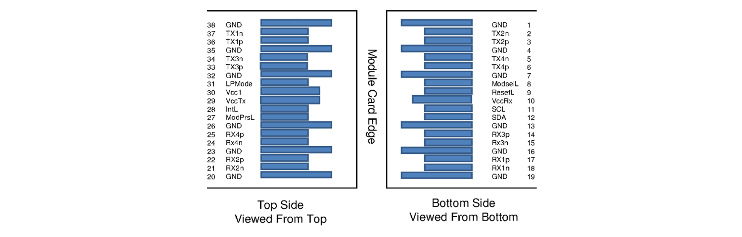
| Pin | Symbol | Name/Description | |||||||
| 1 | GND | Ground | |||||||
| 2 | Tx2n | Transmitter inverted data input | |||||||
| 3 | Tx2p | Transmitter non-inverted data input | |||||||
| 4 | GND | Ground | |||||||
| 5 | Tx4n | Transmitter inverted data input | |||||||
| 6 | Tx4p | Transmitter non-inverted data input | |||||||
| 7 | GND | Ground | |||||||
| 8 | ModSelL | Module select | |||||||
| 9 | ResetL | Module reset | |||||||
| 10 | VCCRx | +3.3V power supply receiver | |||||||
| 11 | SCL | 2-wire serial interface clock | |||||||
| 12 | SDA | 2-wire serial interface data | |||||||
| 13 | GND | Ground | |||||||
| 14 | Rx3p | Receiver non-inverted data output | |||||||
| 15 | Rx3n | Receiver inverted data output | |||||||
| 16 | GND | Ground | |||||||
| 17 | Rxlp | Receiver non-inverted data output | |||||||
| 18 | Rx1n | Receiver inverted data output | |||||||
| 19 | GND | Ground | |||||||
| 20 | GND | Ground | |||||||
| 21 | Rx2n | Receiver inverted data output | |||||||
| 22 | Rx2p | Receiver non-inverted data output | |||||||
| 23 | GND | Ground | |||||||
| 24 | Rx4n | Receiver inverted data output | |||||||
| 25 | Rx4p | Receiver non-inverted data output | |||||||
| 26 | GND | Ground | |||||||
| 27 | ModPrsL | Module present | |||||||
| 28 | IntL | Interrupt | |||||||
| 29 | VCC Tx | +3.3V power supply transmitter | |||||||
| 30 | VCC1 | +3.3V power Supply | |||||||
| 31 | LPMode | Low power mode | |||||||
| 32 | GND | Ground | |||||||
| 33 | Tx3p | Transmitter non-inverted data input | |||||||
| 34 | Tx3n | Transmitter inverted data input | |||||||
| 35 | GND | Ground | |||||||
| 36 | Txlp | Transmitter non-inverted dataInput | |||||||
| 37 | Tx1n | Transmitter inverted data input | |||||||
| 38 | GND | Ground | |||||||


 Ann
Ann


