


|
Product model
|
JFTSM-SFP-GPON-C+2.5/1.25-1413-20-SCS
|
Manufacturer brand
|
JFOPT
|
|
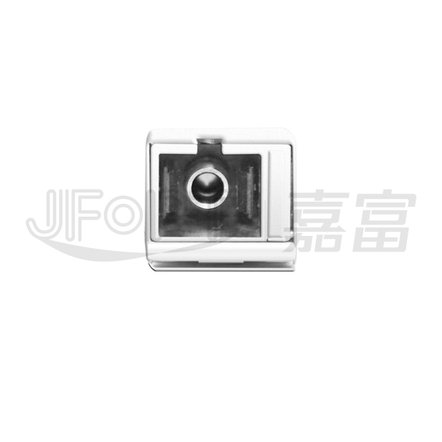
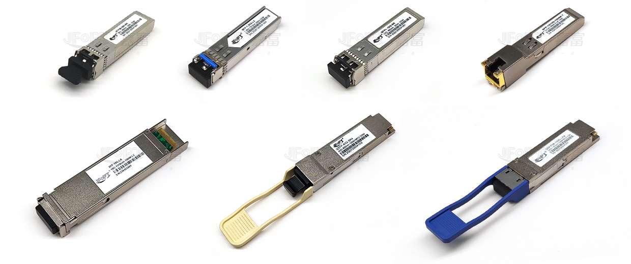
Package type
|
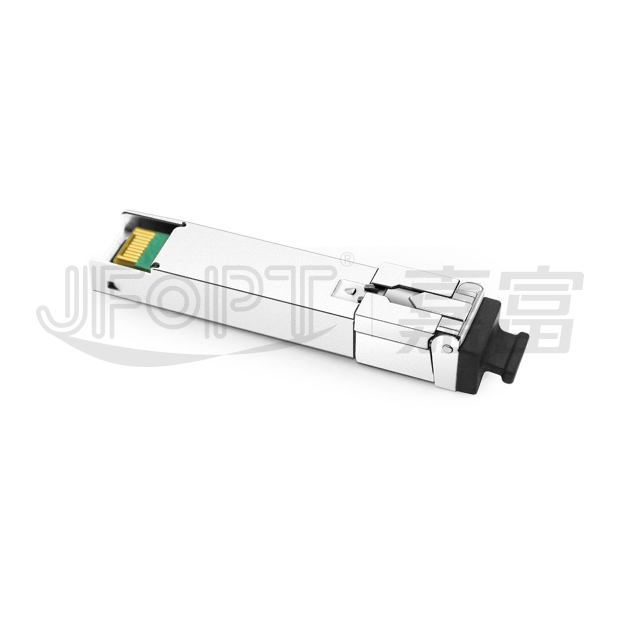
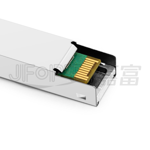
SFP
|
Interface type
|
SC
|
|
Max data rate
|
2.5/1.25Gbps
|
Class
|
C+
|
|
Effective transmission distance
|
20km
|
||
|
Wavelength
|
1310nm/1490nm
1490nm/1310nm
|
Operating voltage
|
3.3V
|
|
Fiber type
|
SMF
|
Core size
|
9/125
|
|
Transmitter type
|
DFB
|
Receiver type
|
APD
|
|
TX power
|
3.5~7dBm
|
Receiver sensitivity
|
-30dBm
|
|
Digital Diagnostic Monitoring(DDM)
|
YES
|
Receiver overload
|
-8dBm
|
|
Power consumption
|
<1W
|
Protocols |
SFP MSA SFF-8472
|
|
Operating temperature(Commercial)
|
0℃~+70℃
|
Storage temperature(Commercial)
|
-40℃~+85℃
|
|
Operating temperature(Industrial)
|
-40℃~+85℃
|
Storage temperature(Industrial)
|
-40℃~+85℃ |
JFOPT continues to invest in optical transceiver production, covering a full range of optical transceiver such as 1*9, SFP, 10G, 25G, 100G, 200G, 400G, 800G GPON/EPON/XG/XGSPON OLT transceiver. At the same time, our company provides TOSA, ROSA, BOSA semi-finished device solutions for the downstream peer. JFOPT's production line has a daily production capacity of 10,000 optical transceivers and 20,000 optical devices. In addition, JFOPT's optical transceiver have industry-leading high temperature resistance and anti-interference capability, and are widely used in computing centers, operators, traffic security, power facilities and other industries.
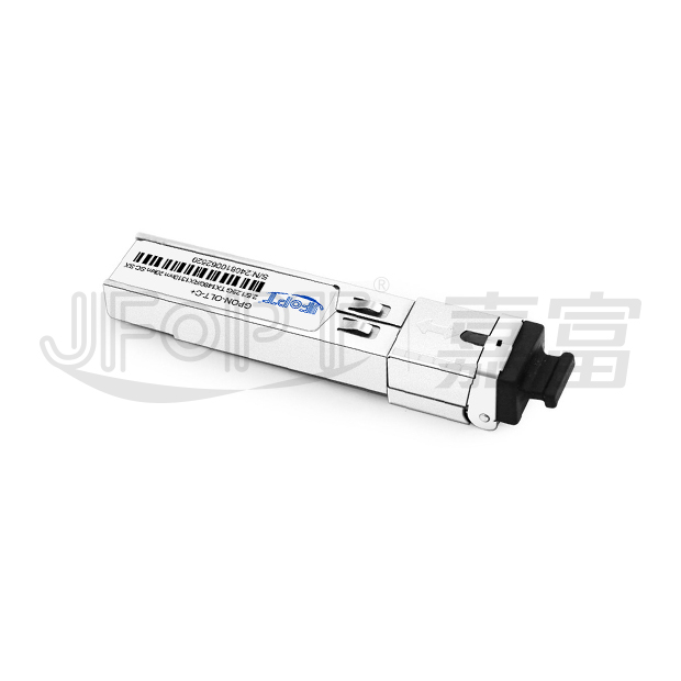
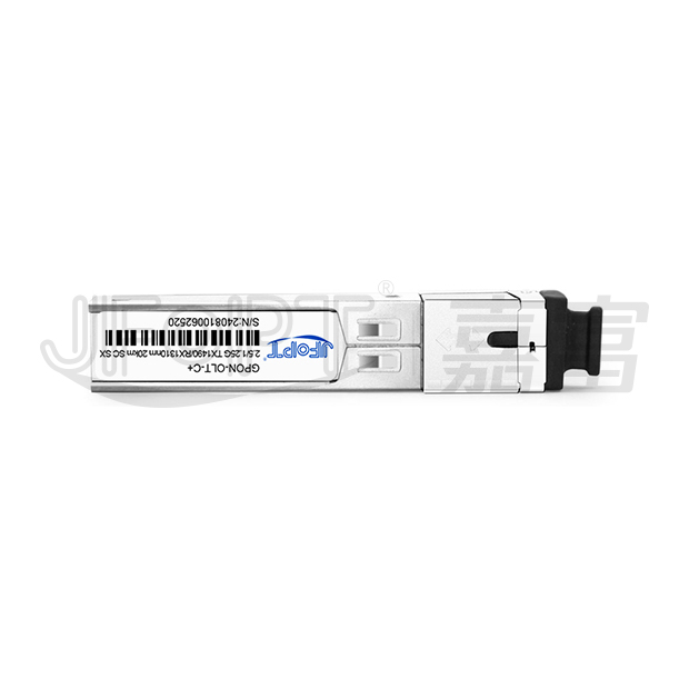
The JFOPT GPON OLT C+ 5dBm Transceiver is an enhanced-performance SFP module engineered for Optical Line Terminals, delivering asymmetric data rates of 2.488Gbps downstream (1490nm) and 1.244Gbps upstream (1310nm) over single-mode fiber with 20km reach. Featuring an SC/UPC connector interface and compliant with the GPON C+ class (5dBm optical budget), this transceiver enables bidirectional communication on a single fiber while supporting Digital Diagnostic Monitoring (DDM) per SFF-8472 for real-time parameter tracking. It fully adheres to ITU-T G.984.2 standards and RoHS requirements.

| Single power supply 3.3V | Small form-factor pluggable (SFP) | ||||||||
| Digital diagnostic monitor compatible with SFF-8472 | SC receptacle optical connector | ||||||||
| Integrated WDM filter for dual wavelength operate at 1490 Tx/1310nm Rx | 1490nm DFB continuos-mode transmitter | ||||||||
| 1310nm burst-mode APD-TIA receiver | LVTTL transmitter disable input and transmitter fault output | ||||||||
| hot pluggable capability | LVPECL compatible data input/output interface |
Gigabit Ethernet Passive Optical Networks (GPON CLASS C+) –OLT side |

| Part No. | Data Rate | Tx Power | Connector Type | Fiber Type | Distance | Temp. | DDMI | ||
| JFTSM-SFP-GPON-C+2.5/1.25-1413-20-SCS | 2.5/1.25G | 3.5~7dBm | SC | Single Fiber | 20km | 0~+70°C | YES | ||
| Parameter | Symbol | Min. | Max. | Unit | |||||
| Storage Temperature | TS | -40 | +85 | ℃ | |||||
| Operating Temperature | Top | 0 | +70 | ℃ | |||||
| Supply Voltage | VCC | -0.5 | +3.6 | V | |||||
| Power Supply Current | ICC | - | 400 | mA | |||||
| Voltage at Any Input Pin | VIN | 0 | Vcc | V | |||||
| Parameter | Symbol | Min. | Typical | Max. | Unit | ||||
| Operating Temperature | Top | 0 | - | +70 | ℃ | ||||
| Supply Voltage | VCC | 3.1 | 3.3 | 3.5 | V | ||||
| Tx Data Rate | - | - | 2488 | - | Mb/s | ||||
| Rx Data Rate | - | - | 1244 | - | Mb/s | ||||
| Parameter | Symbol | Min. | Typ. | Max. | Unit | ||||
Transmitter(T=0 to +70℃, VCC =3.1~3.5V) |
|||||||||
| Central Wavelength | λC | 1480 | 1490 | 1500 | nm | ||||
| Spectral Width | Δλ | - | - | 1 | nm | ||||
| Side Mode Suppression Ratio | SMSR | 30 | - | - | dB | ||||
| Output Power | Po | 3.5 | - | 7 | dBm | ||||
| Extinction Ratio | ER | 8.2 | - | - | dB | ||||
| Output Power at Transmit Off | - | - | - | -40 | dBm | ||||
| Differential Input Voltage | VIH- VIL | 200 | - | 1600 | mV | ||||
| TX Disable Input Voltage Low | TX_DISABLEL | 0 | - | 0.8 | V | ||||
| TX Disable Input Voltage High | TX_DISABLEH | 2.0 | - | Vcc | V | ||||
| TX Fault Output Voltage Low | TX_FAULTL | 0 | - | 0.8 | V | ||||
| TX Fault Output Voltage High | TX_FAULTH | 2.0 | - | VCC+0.3 | V | ||||
| Eye Diagram | Compliance with ITU-T G.984.2 | ||||||||
Receiver(T=0 to +70℃, VCC =3.1~3.5V) |
|||||||||
| Wavelength Range | λ | 1260 | - | 1360 | nm | ||||
| MIN. Input Power (Sensitivity) | PMIN | - | - | -30 | dBm | ||||
| MAX. Input Power (Saturation) | PMAX | -12 | - | - | dBm | ||||
| Signal Detect-Asserted | PA | - | - | -30 | dBm | ||||
| Signal Detect-Deasserted | PD | -45 | - | - | dBm | ||||
| Signal Detect Hysteresis | PHYS | 0.5 | - | 6 | dB | ||||
| Return Loss | ORL | 12 | - | - | dB | ||||
| RX Loss of Signal Output Voltage Low | RX_LOSL | 0 | - | 0.8 | V | ||||
| RX Loss of Signal Output Voltage High | RX_LOSH | 2.0 | - | VCC+0.3 | V | ||||
| LOS Assert Time | TAssert | - | - | 100 | ns | ||||
| LOS De-assert Time | TDeassert | - | - | 12.8 | ns | ||||
| Parameter |
Minimum
|
Typical | Maximum | Unit | Notes | ||||
| RSSI Trigger Delay | 25 | - | - | ns | - | ||||
| RSSI Sampling Time | 300 | - | - | ns | - | ||||
| Internal I2C Delay | - | - | 500 | us | - | ||||
| Receiver Power DDM(RSSI)Error | - | - | +/-3 | dB | - | ||||
| a) RSSI_ACQ input signal rising edge will trigger RSSI sampling, and falling edge will trigger internal digital RSSI information written to I2C. It is recommended that host shall not trigger RSSI_ACQ input again until RSSI data is valid inI2C from previous RSSI trigger. b) RSSI DDM working range is between -8 to -28dBm. RSSI DDM accuracy is better than +/-3dB for input power level between -10 to -28dBm, the accuracy reduces to +/-5dBm to -10 dBm. If the data pattern is at least 2^7-1 or longer, a minimum average of 8 times is strongly recommended to maintain the RSSI reading accuracy. |
|||||||||
| Address | Size (Bytes) |
Name of Field | Hex | Description of Field | |||||
| 0 | 1 | Identifier | 03 | SFP | |||||
| 1 | 1 | Ext. Identifier | 04 | MOD4 | |||||
| 2 | 1 | Connector | 01 | SC | |||||
| 3—10 | 8 | Transceiver | 00 00 00 00 00 00 00 00 | Transceiver Code Field,not applicable | |||||
| 11 | 1 | Encoding | 03 | NRZ encoding | |||||
| 12 | 1 | BR, nominal | 19 | 2488.32Mbps | |||||
| 13 | 1 | Reserved | 00 | Reserved | |||||
| 14 | 1 | Length(9um)-km | 14 | 20(Units of km) | |||||
| 15 | 1 | Length (9um) | C8 | 200(Units of 100 m) | |||||
| 16 | 1 | Length (50um) | 00 | Not Support MMF | |||||
| 17 | 1 | Length (62.5um) | 00 | Not Support MMF | |||||
| 18 | 1 | Length (copper) | 00 | Not Support Copper | |||||
| 19 | 1 | Reserved | 00 | - | |||||
| 20—35 | 16 | Vendor name | XXXXX | “ODI” | |||||
| 36 | 1 | Reserved | 00 | - | |||||
| 37—39 | 3 | Vendor OUI | 000000 | - | |||||
| 40—55 | 16 | Vendor PN | XXXXX | “PART NUMBER ” (ASCⅡ) | |||||
| 56—59 | 4 | Vendor rev | xxxx xxxx | ASCⅡ (“31 2E 31 20” means 1. 1 revision) | |||||
| 60-61 | 2 | Wavelength | 05 D2 | 1490nm Laser wavelength | |||||
| 62 | 1 | Reserved | 00 | - | |||||
| 63 | 1 | CC BASE | xx | Checksum of bytes 0 - 62 | |||||
| 64—65 | 2 | Options | 00 1A | LOS, TX_FAULT and TX_DISABLE | |||||
| 66 | 1 | BR, max | 00 | - | |||||
| 67 | 1 | BR, min | 00 | - | |||||
| 68—83 | 16 | Vendor SN | xxxx xxxx xxxx xxxx xxxx xxxx xxxx xxxx |
SN :xxxxxxxxx (ASCⅡ) | |||||
| 84—91 | 8 | Vendor date code | xxxx xxxx xxxx 20 20 | Year (2 bytes), Month (2 bytes), Day (2 bytes) (ASCⅡ) |
|||||
| 92 | 1 | Diagnostic type | 58 | Externally Calibrated | |||||
| 93 | 1 | Enhanced option | B0 | Diagnostic(Optional Alarm/warning flags) Soft TX_FAULT monitoring implemented Soft RX_LOS monitoring implemented |
|||||
| 94 | 1 | SFF-8472 | 01 | Includes functionality described in Rev 9. 4 SFF-8472 |
|||||
| 95 | 1 | CC_EXT | xx | Checksum of bytes 64 - 94 | |||||
| 96—127 | 32 | Vendor specific | - | Vendor Specific EEPROM | |||||
| 128-255 | 128 | Reserved | - | Reserved for future use. | |||||
| Note: 1.The“ xx” byte should be filled in according to practical case. 2. Note that, A0H is readable and writeable , A2H is readable and write-protected. |
|||||||||
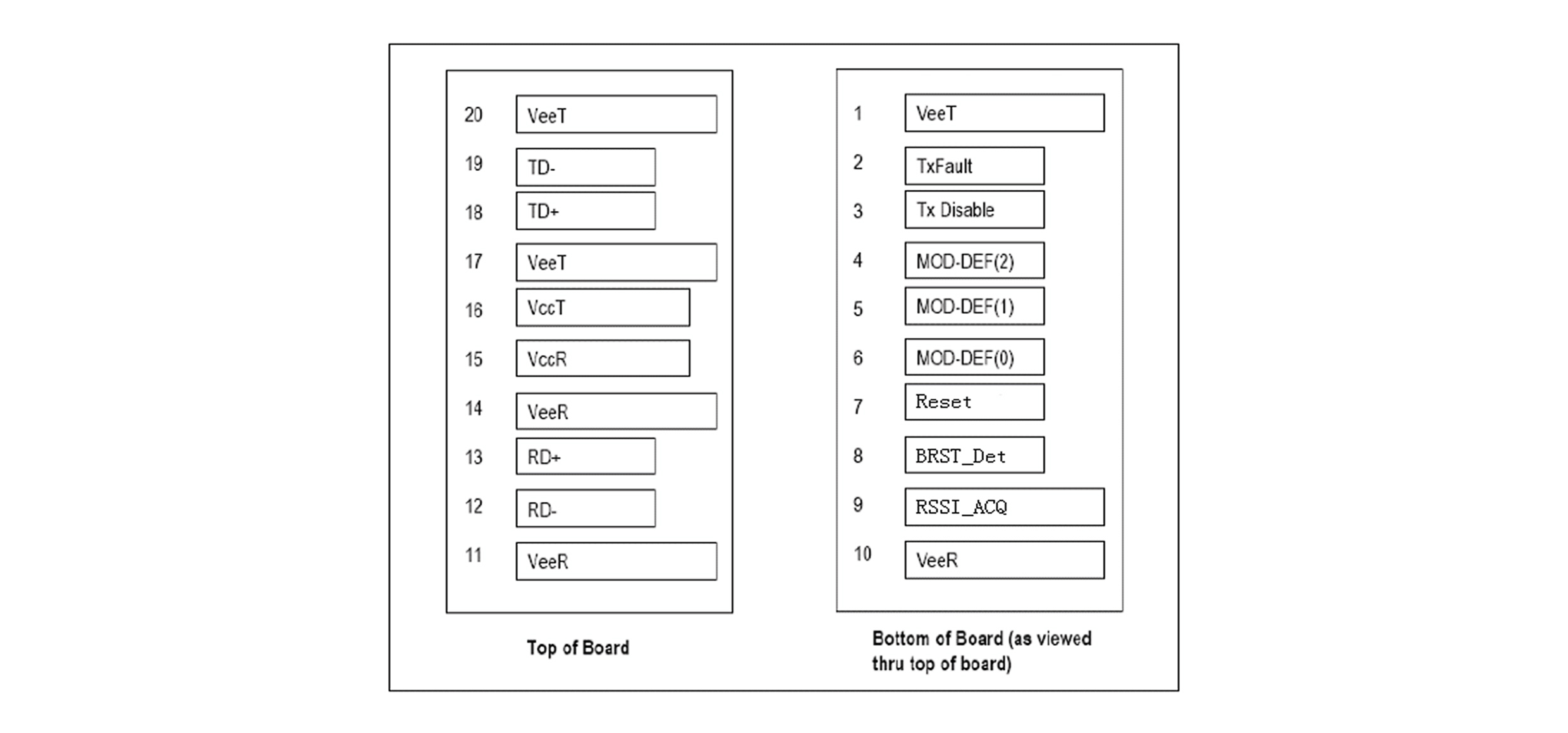
| Pin No. | Name | Function | Plug Seq. | Notes | |||||
| 1 | VeeT | Tx Ground | 1 | - | |||||
| 2 | TX Fault | Transmitter Fault Indication,LVTTL Output Active High | 3 | Note 1 | |||||
| 3 | TX Disable | Transmitter Disable,LVTTL input. | 3 | Note 2 | |||||
| 4 | MOD-DEF2 | 2-Write Serial Data I/O Pin. | 3 | Note 3 | |||||
| 5 | MOD-DEF1 | 2-Write Serial Data I/O Pin. | 3 | Note 3 | |||||
| 6 | MOD-DEF0 | Internally Grounded | 3 | Note 3 | |||||
| 7 | Reset | CMOS input.Assert “Reset” high at the end of previous burst,2 byte in duration | 3 | - | |||||
| 8 | BRST_Det | LVTTL output.BRST_Det assert low when module receives “reset”signal, assert high when incoming burst is present. |
3 | Note 4 | |||||
| 9 | RSSI_ACQ | RSSI acquire/hold LVTTL input. Digital RSSI output through I2C | 1 | - | |||||
| 10 | VeeR | Receiver Ground | 1 | - | |||||
| 11 | VeeR | Receiver Ground | 1 | - | |||||
| 12 | RD- | Inv. Received Data Out | 3 | Note 5 | |||||
| 13 | RD+ | Received Data Out | 3 | Note 5 | |||||
| 14 | VeeR | Receiver Ground | 1 | - | |||||
| 15 | VccR | Receiver Power | 2 | - | |||||
| 16 | VccT | Transmitter Power | 2 | - | |||||
| 17 | VeeT | Transmitter Ground | 1 | - | |||||
| 18 | TD+ | Transmit Data In | 3 | Note 6 | |||||
| 19 | TD- | Inv Transmit Data In | 3 | Note 6 | |||||
| 20 | VeeT | Transmitter Ground | 1 | - | |||||
| Notes: 1. TX Fault is an open collector output, which should be pulled up with a 4.7K~10KΩ resistor on the host board to a voltage between 2.0V and Vcc+0.3V. Logic 0 indicates normal operation; logic 1 indicates a laser fault of some kind. In the low state, the output will be pulled to less than 0.8V. 2. TX Disable is an input that is used to shut down the transmitter optical output. It is pulled up within the module with a 4.7K~10KΩ resistor. Its states are: Low (0~0.8V): Transmitter on (>0.8V, <2.0V): Undefined High (2.0~3.465V): Transmitter Disabled Open:Transmitter Disabled. 3. MOD-DEF 0,1,2 are the module definition pins. They should be pulled up with a 4.7K~10KΩ resistor on the host board. The pull-up voltage shall be VccT or VccR. MOD-DEF 0 is grounded by the module to indicate that the module is present. MOD-DEF 1 isthe clock line of two wire serial interface for serial ID. MOD-DEF 2 isthe data line of two wire serial interface for serial ID. 4. LOS is an open collector output, which should be pulled up with a 4.7K~10KΩ resistor on the host board to a voltage between 2.0V and Vcc+0.3V. Logic 0 indicates normal operation; logic 1 indicates loss of signal. In the low state, the output will be pulled to less than 0.8V. 5. These are the differential receiver outputs. They are AC coupled 100Ω differential lines which should be terminated with 100Ω (differential) atthe user SERDES. 6. These are the differential transmitter inputs. They are AC-coupled, differential lines with 100Ω differential termination inside the module. |
|||||||||


 Ann
Ann


